This is part of a series of blog posts – looking into the appearance and composition of commercially available sharpening stones. If you are interested in the previous episodes, check out the archive for them.
If you have some suggestion on what I should look at next, or want to share your super secret DIY stones, I could be persuaded to open the bag of analytical devices… hit me up on Instagram under @marvgro for that.
Disclaimer: I’m not for sale. Every review you see on this blog is bought with my own money. I have no affiliation to any manufacturer.
Review
Today’s stone is a novel one for this blog. It’s from the Ukrainian company “PT.tools” (also known as PDT or Poltava), which are a manufacturer of abrasive tools. It uses a bronze bond, and the grit chosen (3/2 µm) is perfect for polishing, according to the manufacturer.
Let’s take a look under the microscope!
Optical micrograph of the PTD diamond 3/2 µm. Instrument: Leica Emspira.
The stone is very firm, showing a dark grey colour, that slightly reflects reddish/bronze coloured when the light hits it. Under the microscope, a very even structure is visible. Individual grits are near impossible to make out, because the bronze binder is so reflective.
For a better look, I’ve put the stone into our ultra high resolution scanning electron microscope.
SEM micrographs of the PTD Diamond 3/2 µm. Instrument: Zeiss GeminiSEM560.
The bond is very typical of a dense, highly sintered bronze bond. At the topmost surface, some plastic deformation of the matrix is visible, in deeper recesses some porosity from sintering, but generally speaking this is one dense bond! I typically encounter such tools in my dayjob for precision grinding of glass. The super low concentration of the abrasive also highlights this.
EDS analysis confirms what the manufacturer stats -small diamond grains in a bronze binder. The larger particles visible appear to be Silicon carbide, I’d guess embedded from the dressing process?
EDS analysis of the PTD Diamond 3/2. Instrument: Oxford Ultim Max ∞ 40mm2 EDS sensor. Note that our EDS sensor doesn’t show elements lighter than boron.
Under the focus variation confocal microscope, a relatively smooth surface, dominated by the metal binder and dressing process is visible. This stone will likely create an immense amount of cutting pressure.
Instrument: Bruker Alicona µCMM, 50X objective lens, 3×3 FOV high resolution focus variation scan. Data is leveled and outliers removed (0.25%).
The surface parameters do mirror this finding – a smooth stone with a relatively low surface roughness, and generally dense material ratio (Sdc).
ISO 25178 parameters of the PTD Diamond 3/2 µm.
In order to evaluate the sharpening performance of this stone, a blade was sharpened with it. I am using a standardised testing procedure, read about it here. Nevertheless, it’s 65 HRC M398, and sharpened to 17 DPS with resin bond diamond stones down to 10 µm. Afterwards, the tested stone is used, first in a back and forth movement until the surface becomes homogenous, and then alternating strokes (5-5-3-2) on each side, for a total of 20 strokes towards the apex per side. No pressure is applied but the weight of the apparatus.
The edge is then analysed in the electron microscope for breakouts and morphological appearance.
SEM micrographs of the blade finished with the PTD Diamond 3/2 µm. Deep, regular scratches are visible that were created by the stone.
The sharpening result of this stone was abhorrent. My regular preparation with my own, DrMarv Scientific Sharpening stones leaves a near mirror finish, with a super high gloss at 10 µm. Only by varying the light, some very, very fine scratches can be made out. With the PTD stone, even after just 2 passes, the whole surface turned matte and super dull, with lots of visible scratches. The SEM pictures show this very clearly – with carbide matrix fractures near the apex, and prow formation. It barely did shave, but was easily felt that it’s more tearing and less cutting.
I’m unsure what the issue is here. I would guess that the low concentration and embedded larger SiC particles, combined with the very hard binder mar the surface of the blade. From my professional day job, dressing such a bond is very difficult, requires a quick dressing spindle and low engagement. Nothing that is done easily or cheaply. While grinding with such bonds and concentrations on a milling machine, immense cutting pressure and heat is generated. I wonder why it is made with such a fine grain. If the concentration was bumped by a factor of 10, and large grits were used, it would likely be a fantastic, very long lasting sharpening stone, if the manufacturer was able to integrate some self sharpening properties.
Sharpening disclaimer: I use a standardised approach to sharpening, which basically follows how most manufacturer of guided systems tell you to use this system. I am very aware, that every stone could perform much better than this, in terms of sharpness, but I want a comparable approach. The sharpening segment mostly shows the material removal mechanism – is it burnishing? is it cutting? is the cutting pressure too high so that carbides crack? Is there massive burr or prow formation? The BESS value definitely doesn’t highlight the ultimate sharpening performance of the stone, but was an often requested information. Over time, this blog will show BESS values for different edge morphologies, but by the holy endmill – don’t read it as a “this is the max value this stone can achieve”. I would also suggest to familiarise yourself with the works of Immanuel Kant, it’s absurd I need to write such a disclaimer here.
This is part of a series of blog posts – looking into the appearance and composition of commercially available sharpening stones. If you are interested in the previous episodes, check out the archive for them.
If you have some suggestion on what I should look at next, or want to share your super secret DIY stones, I could be persuaded to open the bag of analytical devices… hit me up on Instagram under @marvgro for that.
Disclaimer: I’m not for sale. Every review you see on this blog is bought with my own money. I have no affiliation to any manufacturer.
Review
Today’s stone is a very famous, well known brand. Naniwa is a Japanese brand, that has been making sharpening stones for over 60 years. Their homepage says they deal in all things abrasive. I like that! The stone I have bought is from the chosera line, with 5000 grit. It is, according to diverse homepages, an alumina-oxide stone with a magnesia binder. Let’s take a closer look:
Optical micrograph of the Naniwa chosera 5000. Instrument: Leica Emspira.
It has some marbeling to it, with a fine and smooth surface. Zooming in, individual particles and grains become visible. For a closer look, as usual, we take a look in the SEM!
SEM micrographs of the Naniwa Chosera 5000 stone. Instrument: Zeiss GeminiSEM560.
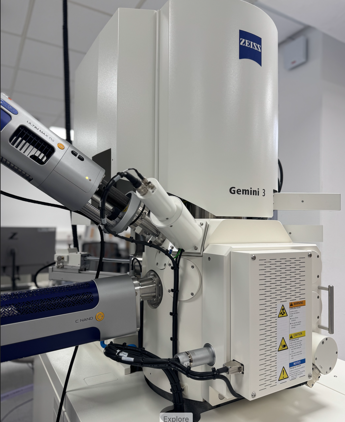
At low magnifications, the stone appears to have a smooth cover above the abrasive grit, covering about 80% of the surface. Zooming in further, one starts to identify cubic, small abrasive grits, but also that the covering “film” actually consists out of an uncountable amount of sub-µm particles, that are slightly rounded and longish. This is an interesting stone! To identify this, we will employ EDS analysis – check out this segment of the blog to understand the SEM metrology better. I mentioned before, that things get… tight once you employ the full suit of sensors. Because this stone is non-conductive, but we need a lot of acceleration voltage to get a reliable EDS reading, I’ve employed our low vacuum mode. With the aid of a small orfice, it is possible to increase the chamber pressure, but leave all sensors functional. For this, a diode-type BSD sensor with the small aperture is inserted pneumatically into the chamber. The EDS sensor meanwhile is shaped like a pen, coming in from the other side. To show you how unbelievably tight and confusing everything gets, I snapped you a shot of the chamberscope:
View from the chamberscope. The stone is visible diagonally from lower left to upper right. The EDS sensor is the pen shaped object coming from the right upper corner. The low-vacuum aperture sits below the pyramidal pole piece, and has been inserted from the left side of the picture. Instrument: Zeiss GeminiSEM560.
The EDS analysis reveals the chemical composition:
EDS analysis of the Naniwa Chosera 5000. Instrument: Oxford Ultim Max ∞ 40mm2 EDS sensor. Note that our EDS sensor doesn’t show elements lighter than boron.
There’s a fascinating mix of chemical elements up there. The old truth “you can find the whole periodic table in ceramics” hold’s especially true. Very interesting is the large particle, with flaky composition. Let’s zoom in a bit more on that one:
SEM micrograph of a flaky particle, found in the Naniwa Chosera 5000 stone. Instrument: Zeiss GeminiSEM 560.
Elemental analysis of the flaky particle. Instrument: Oxford Ultim Max ∞ 40mm2 EDS sensor. Note that our EDS sensor doesn’t show elements lighter than boron.
This is really fascinating! we can pick out what we expected – Mg, O, Al, but also massive amounts of silicon. This is the moment where I am really happy, I haven’t spend more time studying minerals, because I don’t even want to imagine what this could be. Nevertheless, I went on a literature deep dive for you folks. There’s a couple of possibilities this could be – a paper I found had something similar to the flakes we are seeing, but was writen by geologists1. They stated that the flakes they are seeing could either be: Anortit – CaAl2Si2O8; Albit – NaAlSi3O8; and Paligorskit – (Mg,Al)5(Si, Al)8O20(OH)28H2O. The nice thing about geology is, pretty much every mineral has decent SEM pictures online. Albit2 has a matching appearance3, but the excited reader might now ask, where is our Sodium (Na) at this point? Well, it’s pretty exchangeable with Calcium (Ca), which we found in our spectrum. I have no idea what this is called, and I am quite unsure at this point what we found. Structure wise, it should be a triclin crystal latice, and it consists out of the chemical elements Si, Mg, O, Ca. If anyone has studied geology and wants to supply the solution here, reach out. If not, I now declare this to be something like Albit. It doesn’t really matter – it just shows they sinter these stones at quite the high temperature, and there’s cool structures hidden in the microcosmos! All of these oxides are of similar hardness – quite a bit harder than steel, not much harder than carbides.
Let’s take a look at the surface composition!
Instrument: Bruker Alicona µCMM, 50X objective lens, 3×3 FOV high resolution focus variation scan. Data is leveled and outliers removed (0.25%).
It’s a smooth stone, without a large amount of bearing surface. Roughness is not exceptionally smooth, but there are also no super deep recesses. This is a finely made stone, and if you scratch along the surface with your fingernail, there’s nothing catching it. The feedback, because of the relatively rough surface is noticeable. This stone doesn’t glitch over your knife edge.
ISO 25178 parameters of the Naniwa Chosera 5000 stone.
In order to evaluate the sharpening performance of this stone, a blade was sharpened with it. I am using a standardised testing procedure, read about it here. Nevertheless, it’s 65 HRC M398, and sharpened to 17 DPS with resin bond diamond stones down to 10 µm. Afterwards, the tested stone is used, first in a back and forth movement until the surface becomes homogenous, and then alternating strokes (5-5-3-2) on each side, for a total of 20 strokes towards the apex per side. No pressure is applied but the weight of the apparatus. The stone was only splashed with water, not soaked (in accordance with the website I bought it from).
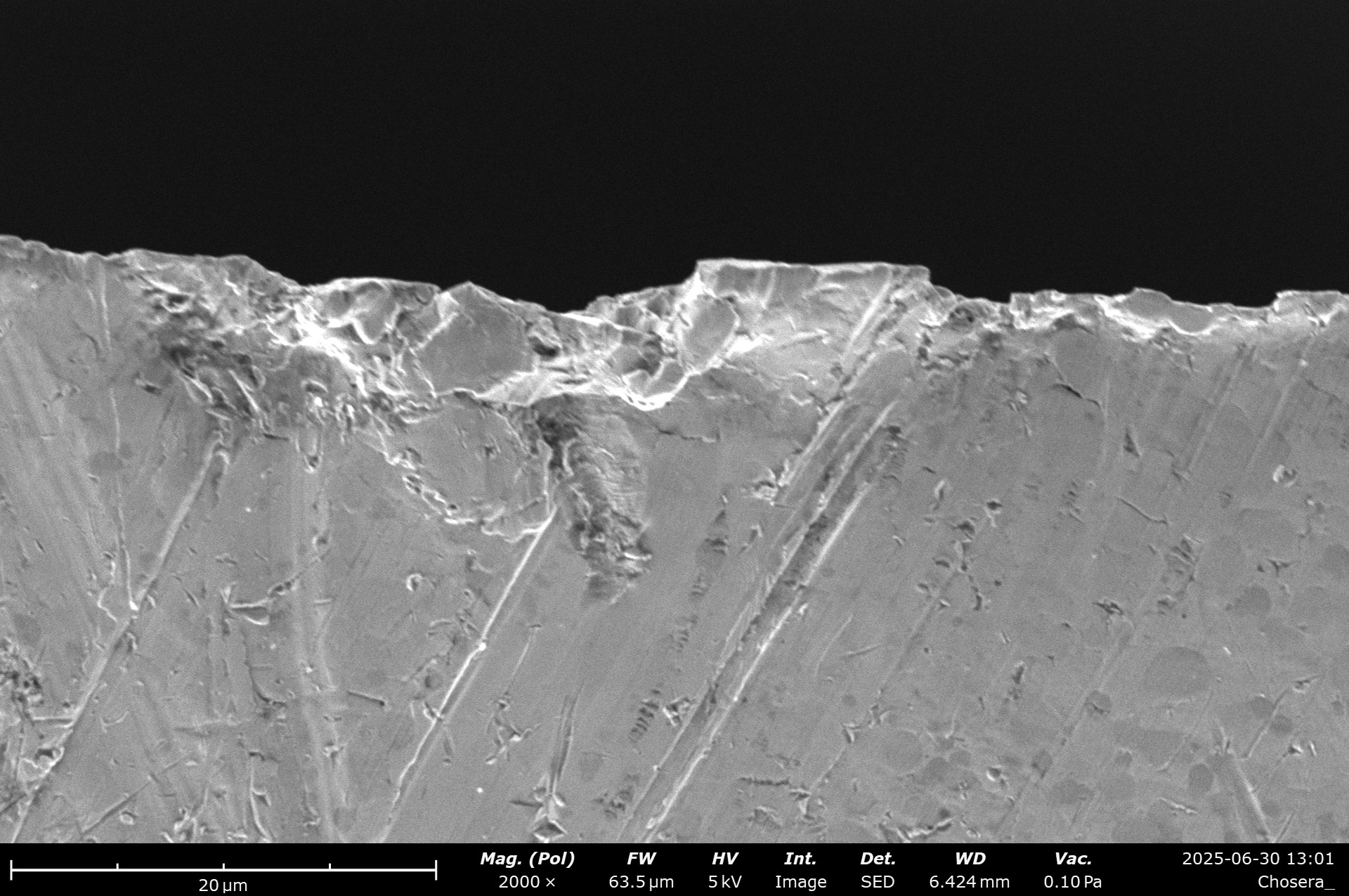
SEM micrographs of the blade finished with the Naniwa Chosera. A slight cross hatch pattern is visible, which stems from me changing hands during the sharpening. The edge is burnished at some parts, whereas other parts show fractures. Overall, the appearance diminished a bit compared to the 10 µm resin stone.
The edge shows no burr, but some cracking near the carbides, brittle failure of the edge and larger scratches are visible. I think the stone struggled a lot with the very hard (65 HRC!) high carbide steel, but also the fact that on a guided system, you can only splash it with water – it doesn’t build up a slurry. Seriously? I think this might be a fantastic stone for freehand sharpening and lower hardness steels. On this guided system, with the minimum amount of water I was able to apply, I am not a super large fan.
I will try to revisit this stone in the future with a softer steel.
References:
Paper: Cvetković, Vesna & Purenović, M.M. & Jovićević, Jovan. (2006). Change of water electrochemical characteristics in contact with magnesium enriched kaolinite-bentonite catalyst substrate. CHISA 2006 – 17th International Congress of Chemical and Process Engineering. ↩︎
This is part of an ongoing blog series about metrology. It explains physics, principles and use cases of modern metrology devices.
TL;DR: Explains how a SEM works. Deep dive into the electron-beam interaction, showing how every sensor gives a different picture and what they could be used for. Lot’s of solid state physics, but in the fun “look at how amazing nature is” way, not in the “equations of horror and despair” way.This should be a fun read and easily understandable, even if you haven’t thought about physics since school.
From the amount of scanning electron microscope (SEM) pictures in this blog, you can guess that I’m a huge fan and heavy user of these wonderful devices.
Brief historical overview& resolution limit
The basic idea behind a SEM is the Abbe diffraction limit of resolution. Ernst Abbe was a pretty cool dude – he lived in Germany during the late 19th century. He defined the foundations of modern optics, had a very impressive beard and is credited with owning Carl Zeiss for some time and the creation of Schott AG. In precision engineering, he has had a lasting impact, mostly for his definition of Abbe Error Compliance (Measurement device in axis of movement is more precise than parallel to axis), but also the Abbe diffraction limit.
It basically states, that the minimum resolvable feature size d is a function of the wavelength of your radiation λ divided by 2 times the index of refraction of the immersed medium n (for example air) times the half-angle subtended by the objective lens θ. The numerical aperture NA describes the resolving power of a objective lens, and is the product of n * sin θ. Thus we have for our system resolution:
d = λ / 2 NA
If you have air between your objective lens and sample, NA can only ever be below 1. Very high quality, large magnification objective lenses can for example have 100x/NA 0.95, coming very close to this theoretical limit. This means, at absolute best, our smallest, resolvable feature is about half the wavelength of the radiation. If you have a nice, confocal microscope, your system might use a green LED at 532 nm, thus your systems resolving resolution is in the range of 0.25 µm. There’s a couple of techniques to get around this limitation, but with visible radiation, you are not going to get massive improvements in lateral resolution. But: the wavelength of radiation is inversely proportional to the energy of the radiation:
E = h*f and: λ = c/f
Visible light typically has an energy of 0.5 – 3 eV, a WLAN signal about 5 µeV. X-Rays start somewhere around 1 keV, and most SEM have their resolution sweet spot at 15-30 keV. Modern tunneling electron microscopes TEM are in the range of 200-300 keV. Sadly, we do not have a TEM at Kern Microtechnik GmbH. *chicken scratches one onto the “Dr.Marv purchase wishlist”*
Now, the actual resolution of a SEM isn’t as close to the theoretical limit as optical microscopy has, because it is surprisingly difficult to compensate all beam and lens (magnetic field) errors. Aberration error correction is something that is only now really hitting the market.
Nevertheless, even a small, entry level desktop SEM like our Thermo Fischer PhenomXL spots a datasheet resolution of smaller than 10 nanometre. Typically, this is achieved as the distance between gold nanoparticles on carbon. Very conductive, maximum elemental contrast and clearly defined boundary edges. It goes without saying, that this is the easiest possible image for a SEM!
SEM micrograph of a very dirty, hydrocarbon contaminated resolution test object. What you see is gold nanoparticles on carbon, at a very high magnification (500kX) and very low accelerating voltage (1 keV). Analysis has shown that our instrument is within specification, even here: 0.7 nm @1keV. Taken with the magnificent Zeiss GeminiSEM560.
At lower energy, the electrons are also much slower, thus experiencing more extraneous influences such as magnetic stray fields or vibrations from body or acoustic noise. A high resolution SEM will have sub 1 nanometre resolution over the entire energy range.
General working principle of a SEM
We have defined that instead of using a beam of visible light, an electron microscope uses a beam of electrons to look at matter. At minimum, an electron microscope consists out of an electron source, some condenser, scanning and focusing “lenses” (which are actually coils with a magnetic field), an aperture, a vacuum chamber with the sample as well as a sensor to detect the signal.
Below is a schematic view of the column design of our ultra high resolution, Zeiss GeminiSEM560.
Schematic cross section of a high resolution SEM column. Pictured detector is a SE2 Everhart Thornley type.
At the electron source, electrons are generated. There’s two typical ways: thermionic emitters, where either a tungsten or a LaB6 filament is heated until free electrons are emitted. The second option is a field emission gun (FEG), where a small filament is heated, but the electrons are removed via a strong electric field. FEG are typically more stable, have less noise and a narrower energy spread. They are more expensive and set higher requirements to the vacuum system.
The electron beam is then accelerated via an electric potential, and then shaped and focused via condenser lenses. The beam current is regulated via an aperture orifice. The beam is then focused and scanned across the sample in a regular pattern via the objective lens. This scanning is not a continuous process, but instead the beam dwells for a short amount of time at every “pixel” position. A detector simply counts the signal emission at every point, thus creating a black and white picture from the sample – electron beam interaction.
It is a very basic principle, but the interaction of the beam and the sample is very complex, and many sensors exist to detect different types of signals. What is really nice about this scanning and way of detecting a picture compared to having a high resolution sensor with many pixels is that all sensors have the same focus point – so you can typically seamlessly switch between sensors and don’t have to refocus.
Electron – Matter – Interaction
In order to understand the different pictures and data created from a SEM, we need to take a quick detour towards high-energy electron beam interaction with matter. When matter is hit with fast electrons (the primary electrons, PE), a couple of possible interactions can happen. The below schematic shows the 4 dominant types, mainly back-scatter electrons (BSE), secondary electrons (SE, type 1 and 2) and x-ray emission (hv). The interaction volume depends on beam energy, but is typically in the range of < 10 nm for SE1, 1-50 nm for SE2, 50-1000 nm for BSE and 1-10 µm for hv. Because of scattering, the interaction volume is shaped a bit like a pear.
Schematic beam interaction with matter. The 4 main emitted signals are shown: BSE, SE1, SE2 and hv.
The interaction volume depends on beam energy, but is typically in the range of < 10 nm for SE1, 1-50 nm for SE2, 50-1000 nm for BSE and 1-10 µm for hv. Because of scattering, the interaction volume is shaped a bit like a pear. To show this interaction, I’ve prepared a small Monte-Carlo scattering simulation highlight this interaction volume, and how deep the different species might reach. This is for a high energy beam in a light material.
Interaction volume of high energy electrons in a light material. SE are highlighted in green.
We will have to dig a bit deeper into the creation of each of these, but also how they change the picture and what data and conclusions we can draw from them. For this, I’ve put a very used, nearly broken carbide end mill into the SEM.
First/left picture: The used endmill, before being inserted into the SEM chamber. Second/Right picture: the inside of the chamber, with the visible polshoe, SE2 detector and illuminated chamberscope. A couple more complex sensors are visible in the background.
After pumping the chamber empty of air, activating the SE2 sensor and focusing, we can generate an overview image of the tool. Because the SEM flares the field at the objective lens, we get a much larger FOV, but heavy distortions. This is mostly useful for navigating and finding a feature (or even: where the heck am I currently!).
SE2 overview picture of the inserted endmill. Instrument: Zeiss GeminiSEM560
Secondary Electrons
Sometimes, when the incident electrons interact with an atom, they do so through inelastic scattering with the shell electrons. This ionises the electron, via ejecting a shell electron, the so called secondary electron. If it’s the primary electron, these SE are called SE1, and are very surface sensitive and detected via a SE detector inside the electron column. If it’s created by backscatter electrons ionising the atoms, they are called SE2 and are detected via an in-chamber detector. These are very sensitive to topography, so the resulting picture is a good representation of the shape and surface of the sample. Because they are created by BSE, the interaction volume is a bit deeper, and the signal can’t resolve very fine surface detail. This sensor is very susceptible to static charge up on the sample.
Schematic depiction of the SE creation process. Note that the incident species can also be BSE, and not only SE.
The SE2 sensor is very fast in it’s readout speed, and typically, especially at longer working distances (distance between the pole piece and the sample) exhibits a strong signal. If the sample is non-conductive, this is my first choice in focusing the picture and for navigating. Because it is at an angle inside the chamber, the sensor gives a very good depth representation of the sample. Pictures look plastic and 3 dimensional.
SEM micrograph of the cutting edge. Signal A = sensor used, in this case the chamber SE2 type. The picture has depth, and nicely shows the morphology of the grinding marks, the coating and particles on the tool.
Switching to the InLens SE1 detector, the picture changes in it’s appearance:
SEM micrograph of the cutting edge. Signal A = sensor used, in this case the InLens SE1 type. The picture has lost some depth, but gained some detail on the surface structure. Besides the grinding marks, the micro-roughness of the coating is now visible.
Because this sensor has a very small interaction volume, it shows fine surface details. Whereas the SE2 sensor mostly showed the grinding path along the tool cutting edge, this sensor shows the micro roughness of the coating, and highlights different sections of the build up edge through finer detail. At the same time, some depth perception is lost, resulting in a flatter picture.
Back Scatter Electrons
Back scatter electrons are created from elastic scattering (reflection) with the nucleus of the atoms. Because of this, the electrons have a lot of energy. The chance for elastic scattering depends on the mass of the nucleus, thus heavier elements give you a brighter signal. Therefore, the BSE signal gives you a material contrast.
Schematic depiction of the SE creation process. Note that the incident species is either the PE, or a lower energy already back scattered BSE.
The same cutting tool we looked at in the SEM can also be visualised with back scatter electrons. For this, our GeminiSEM560 is equipped with two different one: the ESB detector, that sits very high up in the column, and a retractable diode type 4 sector BSD sensor that can be fitted exactly below the pole piece.
Because we can always activate it, let’s start with the ESB detector picture. We can see that the image is flattened a lot – this sensor is not really picking up any topography.
In column ESB detector SEM micrograph of the cutting edge. Note the lighter coloured structures – these are heavier elements than the darker coloured structures.
This sensor is quite “slow”, in the sense of it not getting a lot of signal. The above picture took a bit over 4 minutes to record.
The SEM is fitted with a diode type, 4 sector BSE detector, that can be retracted and inserted via a pneumatic cylinder. Because it is sitting below the pole piece, it is much quicker, and still shows some surface structure.
Chamber BSD SEM micrograph of the cutting edge. The picture has very little depth, showing only a minimal amount of surface structures. The BUE material is clearly distinguishable, showing 2 different materials via the inherent BSD material contrast.
This sensor is much quicker, and shows some topographic details. A bit more depth perception than on the ESB sensor is given.
X-Ray creation (EDS – Energy dispersive x-ray spectroscopy)
The PE are able to create x-rays. I find this absolutely fascinating, and one of my favourite tools inside the SEM. When the PE interacts with the atomic shell, sometimes an electron is ejected (the SE). If this happens at a lower shell, a hole (missing electron spot) is created. Because most systems strive to lower their potential energy, a higher shell electron will then drop down. Because the new orbit has a lower radius, there is now some excess energy. Through this energy, just like Einstein foretold, a particle is created, specifically a x-ray photon. Because the distance between shells is dependent on the weight of the atomic core and it’s configuration (proton number), the energy difference is unique for every element.
Schematic description of the x-ray creation process. An incident electron creates a hole in an inner shell through inelastic scattering (a SE is ejected). A higher shell electron drops down to fill the hole (blue arrow), because of energy conversion the lower orbit energy results in the creation of a x-ray photon.
By recording lots of x-ray photons, and sorting them by their inherent energy, we can identify and map an elemental distribution over our picture. This process is called energy dispersive x-ray spectroscopy. It doesn’t tell you “This is REX 121 steel”, but instead after several minutes you can say “oh, we have about 12 % chromium in our sample. Maybe. I hope. Pinky promise!?”. This is the part where TV shows have ruined science for us scientists. But if done right, at correct readout sampling rates, high beam energy, you get fantastic results.
What can we see on our tool edge? First and foremost the coating material – Ti, Al, N, Cr, resulting from a ceramic high tech multi layer coating applied to most modern tools. Build up edge and particles from aluminum, some stuck carbon, places where the coating has failed and tungsten carbide is visible through the coating. Pretty nifty, eh?
EDS analysis of the tool edge.
The real expertise in EDS is looking at the data and then making judgement calls and drawing from experience and know how. We once found a particle we wanted to analyse, and it contained bromine. People were stumped, because which part of the machine contains bromine? In the end it was the base of our powder coating, and the particle we found at a place it shouldn’t be was the powder coating from the machine enclosure that had flaked off. We managed to nail that down, because the only reasonable expectation of where bromine could be used was exactly that. Comparing a fresh piece revealed identical chemical composition.
Manage Consent
To provide the best experiences, we use technologies like cookies to store and/or access device information. Consenting to these technologies will allow us to process data such as browsing behavior or unique IDs on this site. Not consenting or withdrawing consent, may adversely affect certain features and functions.
Functional
Always active
The technical storage or access is strictly necessary for the legitimate purpose of enabling the use of a specific service explicitly requested by the subscriber or user, or for the sole purpose of carrying out the transmission of a communication over an electronic communications network.
Preferences
The technical storage or access is necessary for the legitimate purpose of storing preferences that are not requested by the subscriber or user.
Statistics
The technical storage or access that is used exclusively for statistical purposes.The technical storage or access that is used exclusively for anonymous statistical purposes. Without a subpoena, voluntary compliance on the part of your Internet Service Provider, or additional records from a third party, information stored or retrieved for this purpose alone cannot usually be used to identify you.
Marketing
The technical storage or access is required to create user profiles to send advertising, or to track the user on a website or across several websites for similar marketing purposes.