Author: Dr Marv

  • A brief study on sharpening stones – Part 6 – Edge Pro Matrix Stone 4000 Grit (5 micron diamond, resin)

    This is part of a series of blog posts – looking into the appearance and composition of commercially available sharpening stones. If you are interested in the previous episodes:

    Part 1 is about the Fällkniven DC3 , Part 2 is about the DMT mini W7C, Part 3 is about the TSPROF Blitz F1000, Part 4 is about a natural jade stone, Part 5 is about the Venev 5/3 Diamond Resin Stone.

    If you have some suggestion on what I should look at next, or want to share your super secret DIY stones, I could be persuaded to open the bag of analytical devices… hit me up on Instagram under @marvgro for that.

    Today’s sharpening stone is the Edge Pro Matrix Stone at 4000 grit, which according to the manufacturer equals 5 micrometre grain size. It’s their stone “made for modern super steel” and apparently self sharpening by loosening grains over time. 🙂

    It’s a super smooth, very fine stone. Stroking it with your finger, it just feels barely sticky, while scratching it with your fingernail shows some resistance – but can also leave a small groove.

    Optical micrographs of the Edge Pro Matrix Stone (4000). The scale bar is visible in the lower right corner. Instrument: Leica Emspira.

    The microscope supports this picture. A very uniform, smooth surface. The corners around the stone are slightly beveled. At higher magnifications, grains start to become visible. Do we have a new king of agglomeration here? Let’s throw it into the SEM to check it out.

    The first thing I saw in the SEM was…nothing. Because this stone is so smooth, and also because they really seem to use no fillers, additives or anything else, it immediately starts charging like crazy. The resin they are using is also covering the topmost layer, making it hard to distinguish between resin and diamond. Well, this ain’t a BEAST of a scanning electron microscope for nothing. We’ve equipped it with multiple sensors and it is a very versatile device. To make an image visible, I’ve bumped up the accelerating voltage. To explain why this is different to the other pictures you’ve seen in this blog before, I think I need to detour for a small moment.

    In a scanning electron microscope, the image is created by using a beam of electrons, and moving that one in regular lines across the surface of a sample. At every point it hits the sample, interaction happens. This interaction is typically either an elastic reflection of the incident electrons (back scattered electrons, BSE), or the ejection of electrons from a shell around the atoms (secondary electrons, SE). The BSE are showing you mostly elemental contrast, whereas the SE show you a topographical (surface) contrast. Nevertheless, with good enough sensors, both show you a bit of the information of the other type. Now, the BSD (back scatter detector) is pretty robust, and works nicely at lower vacuum. Because the sample is non conductive, it will experience static charge. Lowering the chamber vacuum introduces moisture (H2O) into the chamber, and this is enough to reduce the static charge on the sample. Unfortunately, lower vacuum also means lower resolution, and the BSD doesn’t give us great surface morphology to begin with. A workable way to combat this is to increase the accelerating voltage. This will not only give you more signal, reduce noise, but also increase the interaction volume of the beam. Basically, you are now looking a couple micrometre deep into the material!

    SEM Micrographs of the Edge Pro Matrix Stone (4000). Note that these pictures are BSD and at high accelerating voltage. Instrument: Zeiss GeminiSEM560.

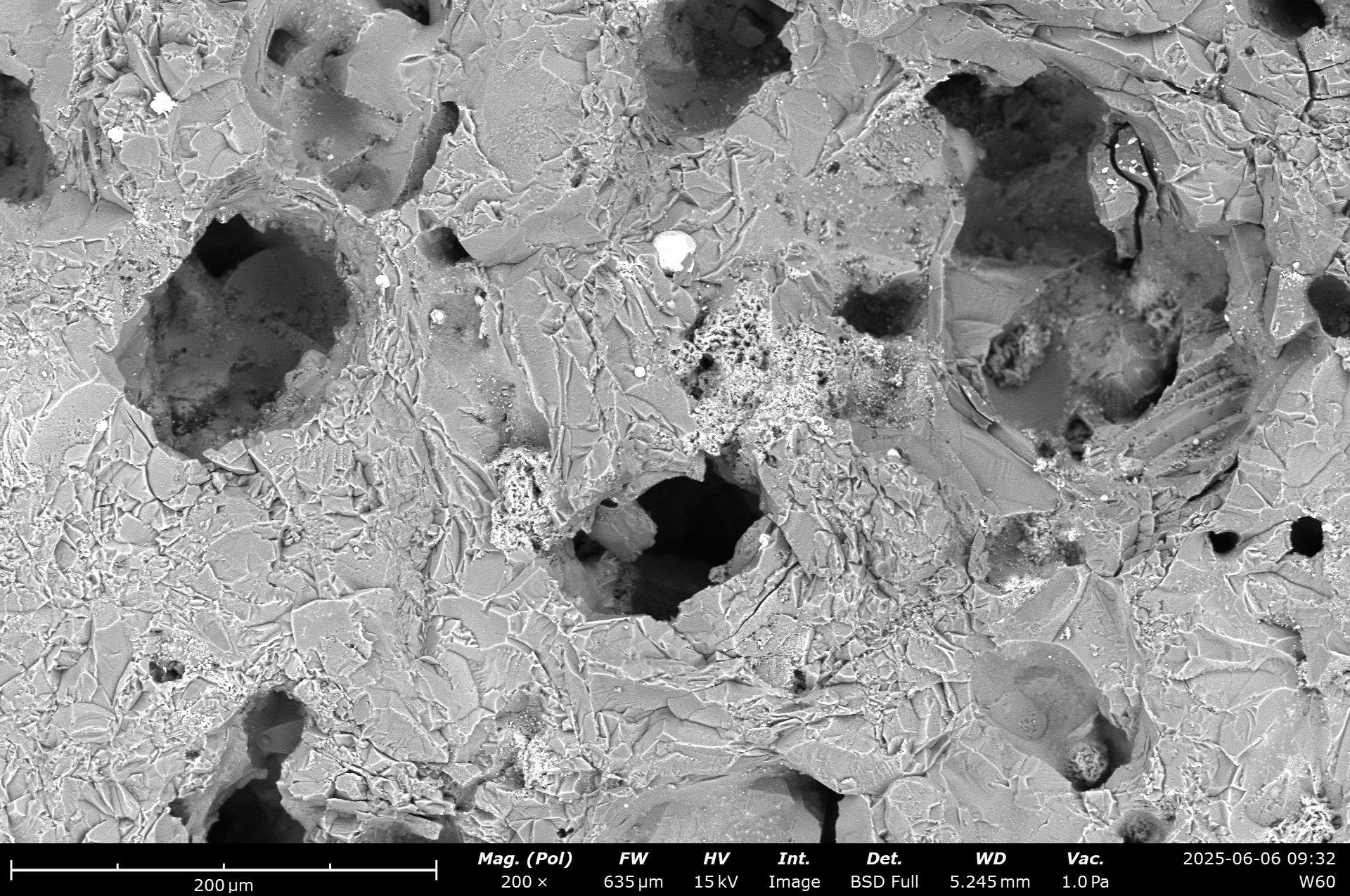
    We can see that this stone really only contains a matrix and the diamond grit. All grains are small with tight controlled size distribution. No fillers or other abrasives are visible. The matrix is relatively dense, and the atomic contrast of it is similar to the diamond next to it. This is the first stone I’ve looked at that contains no fillers. Unfortunately, with this comes two problems: Quite a bit of agglomeration is visible, with often 3 or more grains sticking close to each other. The second is the retention of the grains – we can see on this unused stone already, that nearly no grain is sticking out of the surface. Even the manufacturers dressing process removed the majority of all surface grains. I would expect this stone to be quite slow and soft. Because of the simple composition, no EDS was recorded.

    The surface under the white light interferometer shows a smooth, regular and low roughness surface.

    White light interferometry height map of the Edge Pro Matrix Stone (4000). Instrument: Zygo Nexview NX2, Objective Lens: 10X. Stitched overview of 4×4 images.

    The overall height distribution is lower than for example on the similar grit Venev stone. The actual contact surface, at least brand new, should be relatively low, as it doesn’t show a lot of plateaus in the height map.

    ISO 25178 parameters of the Matrix Pro Stone (4000).

    The areal surface parameter support this observation. This is one very smooth stone, with very low roughness and material ratio.

    In order to evaluate the sharpening performance of these stones, 3 blades were sharpened. In order to evaluate the sharpening performance of this stone, a blade was sharpened with it. I am using a standardised testing procedure, read about it here. Nevertheless, it’s 65 HRC M398, and sharpened to 17 DPS with resin bond diamond stones down to 10 µm. Afterwards, the tested stone is used, first in a back and forth movement until the surface becomes homogenous, and then alternating, edge trailing strokes (5-5-3-2) on each side, for a total of 20 strokes per side. No pressure is applied but the weight of the apparatus. Then the Pro Matrix stone comes into play.

    SEM micrographs of the sharpened blade. Note that the last picture (2kx magnification) isn’t a center zoom of the one before, but slightly to the left of the FOV, as I identified some carbide cracking that I wanted to visualise in higher detail. Instrument: Thermo Fischer PhenomXL Scanning Electron Microscope.

    The surface of the edge is much smoother than with the equally sized Venev sharpening stone. The edge shows a low waviness and no identifiable burr. This is certainly a statement to the heat treat of the steel (made by Roman Kasé!), but also to the stone. Some deeper grooves are visible, which could be because of the agglomeration, or a rolling grain that got loose. The low material removal rate gives a high cutting pressure, likely leading to the carbide cracking and edge breakouts at carbide-steel interfaces. This is a cool stone, with a nice feeling while sharpening, awesome result and very finely made. I like it. If only it was a faster stone!
  • A brief study on sharpening stones – Part 5 – Venev Double Sided Diamond Stone 5/3 Side

    A brief study on sharpening stones – Part 5 – Venev Double Sided Diamond Stone 5/3 Side

    This is part of a series of blog posts – looking into the appearance and composition of commercially available sharpening stones. If you are interested in the previous episodes:

    Part 1 is about the Fällkniven DC3 , Part 2 is about the DMT mini W7C,

    Part 3 is about the TSPROF Blitz F1000, Part 4 is about a natural jade stone.

    If you have some suggestion on what I should look at next, or want to share your super secret DIY stones, I could be persuaded to open the bag of analytical devices… hit me up on Instagram under @marvgro for that.

    Today’s sharpening stone is an artifical, resin bound diamond stone. I believe these are sold under the TSPROF brand, but are made by Venev and are made by Venev, too. While it has two sides, for comparisons sake I only looked at the 5/3 micron side in detail. Why does it have two numbers here? Well, getting a very tight control on the grain size is expensive. Up to a certain size one can sieve it, and there you’d obviously have a spread of sizes (basically: everything that was smaller than the last sieve you used, but larger than the current sieve you are using). At a certain grit size though, this process is replaced by sedimentation. You basically dump your diamond powder that is created by crushing larger diamonds against each other into a tank with water, stir it vigorously and then leave it standing. Heavier particles sink to the bottom quicker than lighter ones, so you then suction it off layer by layer. The more careful and skilled one is at this process, the tighter the size distribution is. Typically, asia-sourced diamond is pretty good at this. Nevertheless, 5/3 is a very honest way of describing it. In Germany, tightly controlled (and lab analysed & certified!) diamond powder is readily available, but about 20 times more expensive than foreign sourced one. We should therefore expect to have a wide range of different grain sizes in this stone.

    Taking a look under the optical microscope, a mix between reflective grains, darker but also green grains and a reddish matrix is easily identifiable.

    Optical micrographs of the Venev double sided 5/3 micron diamond stone. The scale bar is visible in the lower right corner. Instrument: Leica Emspira.

    It would be quite interesting to see what grains are diamond, what the other ones are (or if all are diamond!) but also what the surface microstructure looks like. For this, the scanning electron microscope is king. The resolution and depth of focus is just so nice. As this is a 1″x6″ stone, off it goes into our fantastic Zeiss GeminiSEM560. Absolute overkill, but it fits, so we here we go:

    SEM Micrographs of the surface morphology of the Venev 5/3 micron diamond stone. Instrument: Zeiss GeminiSEM560.

    The manufacturer says that they are using an organic bond, based on phenol-formaldehyde resins. These are typically improved by adding various fillers to them, for example SiC (to make it harder), copper (to improve heat transfer), but also organic material such as woodchips or fabric fibre to improve tensile strength. Information from the manufacturer about this is a bit inconclusive – apparently, they have a “B2-01” bond, that has fillers, and an improved “OSB” bond, that should not have “boron carbide” in it. Apparently the finer stones, such as this one, have the improved bond. What I find curious at this point is that the above SEM pictures show a large variance of grains – some, that would fit in the 5/3 micrometre range, but others that are much larger, and of a lighter colour. The SEM is special in terms of microscopes, in that every picture not only contains topographical information (e.g. the surface appearance), but depending on the sensor also some chemical information. The sensor used for the pictures above is the “SE2” sensor, which detects secondary electrons. These are created in the beam-matter interaction by basically hitting an electron on the atom-shell, and shooting it out. It is a very surface sensitive detector, mostly showing topography. Nevertheless, if you have much heavier elements, you get a very slight elemental contrast. The large grains are slightly lighter grey than the smaller grains, which could point towards them consisting out of heavier elements, for example SiC instead of C which would be found in pure diamond.

    Fortunately, the SEM is equipped with a sensor to identify elements.

    EDS analysis of the Venev 5/3 micron diamond stone. Instrument: Oxford Ultim Max  ∞ 40mm2 EDS sensor. Note that our EDS sensor doesn’t show elements lighter than boron.

    As postulated above, the abrasive in this stone consists out of some large, 10-15 micrometre sized silicon carbide (SiC, pink colour) grains, but also some agglomerated magnesium-oxide particles (MgO, green colour). The diamond grain concentration looks to be about C100 (equaling 25% by volume, but the standard is pretty vague on how and when this is determined). Nevertheless, I’m a bit disappointed by the mixing here – it seems like we have several agglomerated nests of diamond, with some spare grains in between. Also, I would imagine one will have quite the large scratches from the large SiC particles. SiC typically reaches a hardness of 2500-3000 HV, much harder than a decent powder metallurgical steel would achieve (64 HRC are around 800 HV, CBN is at 4000-5000 HV, diamond at 10000 HV in it’s hard crystallographic orientation). MgO meanwhile comes in at 1200 HV. In subtractive manufacturing, the typical rule of thumb is: your abrasive should be 5 times harder than the workpiece. Otherwise, you will have excessive wear on it. The binder clearly is organic in origin, a phenol based one seems likely by the appearance and “brittleness” of it. If you ask me, this was baked at a bit too high of a temperature, and with not enough pressure. This could explain the “debris type” dusting on it, as well as the large voids.

    Taking the stone for a look under the white light interferometer, we can see the surface structure is very regular, but also quite coarse.

    White light interferometry height map of the Venev 5/3 micron sized stone. Instrument: Zygo Nexview NX2, Objective Lens: 10X. Stitched overview of 5×5 images.

    I could imagine that the deep pits we are seeing are actually foaming of the phenol-resin during the curing process, and not just tear outs from the dressing process, as I haven’t identified any particles this large. Nevertheless, if you compare it with the SEM picture of the large, molten agglomeration of binder, it could also be that these are distributed all along the stone, and we see the result of these tearing out.

    ISO 25178 parameters of the Venev 5/3 micron diamond stone.

    The stone is actually, and quite surprisingly, very coarse in it’s surface. I would have expected a stone with this fine grit to have a fine, polishing surface. The roughness is actually much higher than on for example the natural jade stone we looked at the last time. Nevertheless, the shape of the surface in itself can’t be considered very sharp, as for example the Kurtosis (Sku) is only slightly above 3.

    Seeing as this is an interesting stone for sharpening, I’ve taken the trouble of sharpening a blade with this. In order to evaluate the sharpening performance of these stones, 3 blades were sharpened. In order to evaluate the sharpening performance of this stone, a blade was sharpened with it. I am using a standardised testing procedure, read about it here. Nevertheless, it’s 65 HRC M398, and sharpened to 17 DPS with resin bond diamond stones down to 10 µm. Afterwards, the tested stone is used, first in a back and forth movement until the surface becomes homogenous, and then alternating strokes (5-5-3-2) on each side, for a total of 20 strokes towards the apex per side. No pressure is applied but the weight of the apparatus. Then the Venev stone was used.

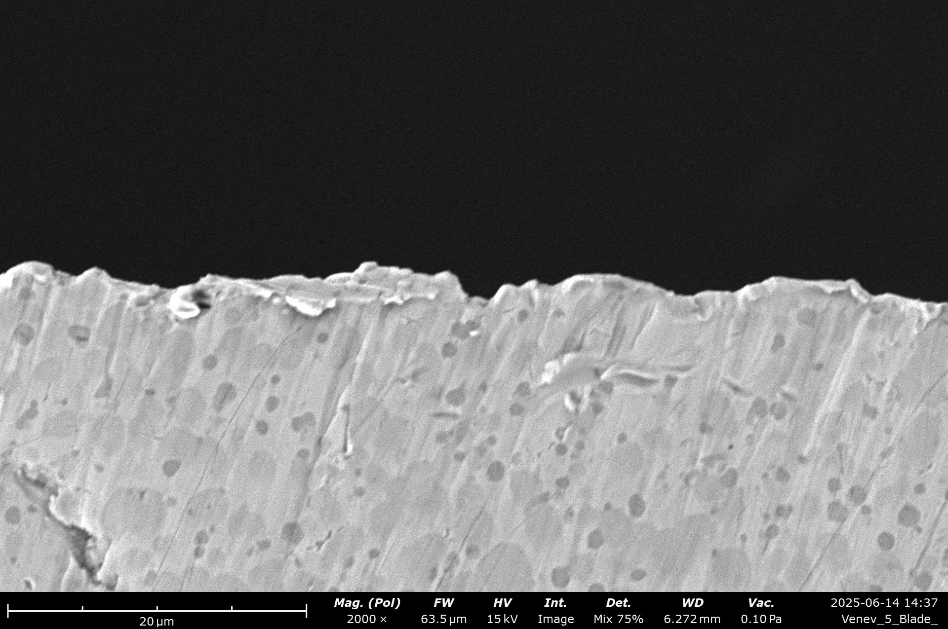
    SEM micrographs of a test blade, done with the Venev stone. Note the beautiful distribution of carbides in the M398. Boehler and Mr. Kasé are magicians! Instrument: Thermo Fischer Phenom XL Scanning Electron Microscope.

    The result is a keen edge, with burrs that are already very hard to detect under an optical microscope. The largest burr I found was in the low, single digit micrometre range. Nevertheless, there’s some heavier scratches, and the cutting edge is slightly wavy. Comparing the deeper pits at the edge, I don’t think it’s massive carbide cracking, as those are a bit larger than the very fine carbides. I would imagine this is most likely the larger SiC grains, grinding away the edge. A pity!

  • A brief study on sharpening stones – Part 4 – natural Jade

    This is part of a series of blog posts – looking into the appearance and composition of commercially available sharpening stones. If you are interested in the previous episodes:

    Part 1 is about the Fällkniven DC3 ,

    Part 2 is about the DMT mini W7C,

    Part 3 is about the TSPROF Blitz F1000.

    If you have some suggestion on what I should look at next, or want to share your super secret DIY stones, I could be persuaded to open the bag of analytical devices… hit me up on Instagram under @marvgro for that.

    Today’s sharpening stone is a natural jade stone. Jade is a natural occurring stone, that consists out of complex silicates. I believe that typically the one used for sharpening is from the pyroxene group. There, the minerals consist out of a certain formula: (XY(Si,Al)2O6) where X typically is a light metal such as Calcium, Sodium and Y typically is a heavier metal such as aluminium, chromium. I mention this, because jadeite typically is not pure NaAlSi2O6, but more likely a wild and varying mix of several elements, some maybe only in traces. Nevertheless, silicates are hard, with jadeite typically reaching around 1000 HV. This is harder than a cheap knife, but actually softer than some high carbide steels at their maximum achievable hardness. The other mineral that is commonly called jade is nephrite, which is a really complex mix of Ca2(Mg,Fe)5Si8O22(OH)2.  This is typically a bit softer, ranging from 700 to 1000 HV (hardness vickers). We’ll see whether we can identify what mineral our natural jade stone is made of later!

    Taking a look under the optical microscope, it is clearly identifiable as jade by it’s distinct, swirly white and green colour:

    Optical micrographs of a natural jade stone. The scale bar is visible in the lower right corner. Instrument: Leica Emspira.

    One can make out some distinct silicate grains, with a more whitish colour, and also some darker debris, likely swarf stuck to the surface. Jadeite is non-conducting, so we once again get to enjoy absurdly detailed pictures from the fantastic Zeiss GeminiSEM560. Because of it’s design, it excels at low voltage imaging, where one has lower charging effects.

    SEM Micrographs of the surface morphology of the natural jade stone. Instrument: Zeiss GeminiSEM560.

    The SEM pictures reveal a ragged topography, consisting out of a mix of ultra fine, debris like grains, but also larger, well formed grains. I struggle to give this stone a classification in terms of grit – the grains are sometimes in the nanometer range (compare the 2KX magnification picture), but some are also several micrometre large, up to maybe the low double digits.

    A nice question here is: what type of jade is this actually made out of? For this, we employ the EDS module of the Zeiss GeminiSEM560. With energy dispersive x-ray spectroscopy (typically abreviated EDS or EDX), one can identify the elemental composition of a SEM sample. This doesn’t mean you press a button and crime show like you get a beep and it identifies the material. It means that after a couple minutes, with the uncertainty of a couple percent, you can state “I think it contains iron. maybe.”. Welcome to science!

    EDS analysis of the natural jade stone. Instrument: Oxford Ultim Max  ∞ 40mm2 EDS sensor. Note that our EDS sensor doesn’t show elements lighter than boron.

    It’s generally a good idea with EDS analysis to compare the composition in percent (visible in the second picture above) with the colour map of where these elements appear. As the “full colour” summary image is quite hard to differentiate, I typically use that one to pick out the area or grain of interest, and then peek to the smaller, individual colour slices. EDS analysis nicely identifies that this jade stone consists out of Ca, Mg, Si, O. These are the elements found in neprhite (Ca2(Mg,Fe)5Si8O22(OH)2), so it’s pretty safe to say this is what the stone is made out of!

    One really cool thing our Zeiss is equipped with is a sensor called “VPSE”. This stands for variable-pressure, secondary electron detector. It doesn’t detect electrons directly, like a Everhart-Thornley would. If your sample is in “low vacuum” conditions, that ET-SE detector would short circuit out because the air is conducting. Nevertheless, secondary electrons are created by the electron beam-matter interaction, and those create little light flashes when they hit molecules in the low atmosphere at VP. Now, the VPSE detector has a very sensitive scintillator that detects these flashes. I’m telling you this, because if you aren’t in low vacuum, and you have a mineral sample, you can use the VPSE as a cathodoluminescence detector. Here, the electron beam sometimes creates light in the interaction with certain minerals. Sadly, with “abusing” the sensor in this way, it’s still only a black and white picture. But if your sample glows, you can make that visible.

    “abused” VPSE sensor micrograph to highlight cathodoluminescence of the jade stone. Image FOV is identical to the SE2 image earlier in this post. Instrument: Zeiss GeminiSEM560.

    Does it have any relevancy to this post? No. Is it super awesome and cool? Yes!

    In order to look at the surface of the stone, the awesome Zygo Nexview NX2 white light interferometer comes to use again:

    The jade stone while being measured on the Zygo Nexview NX2 interferometer.

    The stone shows a relatively smooth surface. The uppermost surface is actually pretty flat, with a large material ratio (bearing surface). Some deep voids are sprinkled randomly over the surface.

    White light interferometry height map of the jade stone. Instrument: Zygo Nexview NX2, Objective Lens: 10X. Stitched overview of 5×5 images.

    The high material ratio with a smooth surface is one reason why this stone feels nearly like glass – very little feedback, as the contact surface area is large, and the knife slides along it without really grabbing onto the grains. This is a stone for very low removal and mostly I would guess it burnishes a knife edge.

    ISO 25178 parameters of the natural jade stone.

    Roughness wise, this is a pretty coarse stone (Sq > 7 µm), with a sharp profile (Sku, kurtosis >> 3). Nevertheless, the topmost surface is ground pretty flat.

  • A brief study on sharpening stones – Part 3 – TSPROF Blitz F1000 (Extra Fine, Galvanic Diamond)

    This is part of a series of blog posts – looking into the appearance and composition of commercially available sharpening stones. If you are interested in the previous episode, Part 1 is about the Fällkniven DC3. Part 2 is about the DMT mini W7C

    If you have some suggestion on what I should look at next, or want to share your super secret DIY stones, I could be persuaded to open the bag of analytical devices… hit me up on Instagram under @marvgro for that.

    Today’s sharpening stone is actually one in two conditions. I recently aquired a TSPROF K03 Pro Hunter sharpening system. After DIY-messing-it-up twice to make a similar system and loosing the wish to continue sharpening knifes over the past decade, I decided it’s time to go for another round in the why-is-this-not-electric-powered. Or maybe my friend Roman Kasé bought one, and I generally try to imitate the master of steel as much as I can when it’s about sharpness. 🙂

    The Blitz F1000 is a galvanic bound diamond grinding stone. Yes, we are noticing a pattern here. Why are there so many galvanic bound stones? Generally, because they are dirt cheap to make. Let me share the process by which you create galvanic bound stones with you: First, you take a metal substrate that is conducting. You sprinkle some diamonds on top. Then you immerse it in a (typically blue) solution containing nickel-ions, apply some voltage for a couple of minutes. The first growth of the electro-deposited nickel matrix starts away from the stone, as that one functions as part of your anode-cathode system. After a short amount of time, you remove it, brush off the excess diamond (only the submost layer will stick if you time it right!), transfer it into a second bath of nickel-solution, and continue the electrodeposition for a couple more minutes. The whole process is ghastly unhealthy, energy intensive and cheap enough that even in Germany companies are producing grinding media this way.

    Now, the TSPROF F1000 is the “finest” of the galvanic bound diamond stones in the TSPROF set of 5 stones. The grit, according to the manufacturer is 1000, which should be somewhere in the range of 17 µm. This is already very fine and quite difficult to make on galvanic bound grinding media.

    Optical micrographs of a brand new TSPROF Blitz F1000. The scale bar is visible in the lower right corner. Measurement Instrument: Leica EMSPIRA.

    Optical micrographs show a smooth, regular surface with slight dents and fractures along the circumference and the edges. This doesn’t hurt the function, and I think the corner might also be from me, using it to scratch in a part number on a blade I was sharpening…

    The real magic is revealed inside the SEM, as usual. Unfortunately, 6″x 1″ large grinding stones don’t fit into the desktop SEM we have, so the “big one” has to come to the rescue. The upside for you: pictures are so much better. This is taken on the Zeiss GeminiSEM560, a ultra high resolution field emission gun scanning electron microscope, featuring a nano-twin lens that combines the magnetic and electrostatic field into the last lens. If you get really close, this beast has sub-nanometre resolution across the whole voltage spectrum. Resolution improves over the desktop model by nearly 3 orders of magnitude. It’s likely the most expensive SEM you can buy, and probably the first time one of these sees a knife grinding stone 🙂 The magnification is defined identically to our other SEM (polaroid standard comparison), so you can easily cross reference with previous (and future) blog entries from the other SEM.

    SEM Micrographs of the surface morphology of the unused TSPROF Blitz F1000 sharpening stone. Microscope: Zeiss GeminiSEM560.

    The SEM micrographs reveal quite the even spacing between grains. Some are embedded very far, whereas others are peaking out massively. In my professional opinion, this is the result of someone who has a very decent workflow in preparation (spacing), but struggles with the very fine grain size. Grain size distribution is pretty even, and the grains are very sharp and flat ones. This is one hell of an abrasive stone. Good thing it’s meant to do abrasion!

    White light interferometry height map of the diamond surface. Instrument used: Zygo Nexview NX2, Objective Lens: 10X. Stitched overview of 4×4 images.

    White light interferometry looks a bit weird at first glance. In the SEM pictures, the grains weren’t this densely packed together. It shows large regions with higher and lower parts, but the difference between these should be measured in low single digit µm. This is likely height variations of the matrix we are detecting here! Zooming in a bit into the overview reveals the actual grains:

    White light interferometry height map of the diamond surface. Instrument used: Zygo Nexview NX2, Objective Lens: 10X.

    Fortunately, the ISO 25178 parameters are, while dependent on the area you select, pretty robust. Once you capture around 40 roughness creating events in every direction, your parameters don’t change a lot, and we can get away with a single parameter table this time.

    Unsurprisingly, this is the smoothest stone with the lowest numbers so far. Even if you were to directly “imprint” the surface of this stone onto your knife, your surface roughness would be just above 1 µm. That’s often a challenge in steel for mediocre milling machines. The edges made by this stone are, while not glossy, already very fine, sharp and shiny.

    In the beginning of this post, I teasered that this stone will be featured in two conditions – and the second is obviously, used! I’ve sharpened a grand total of 4 blades on it – 3 from M398 at 68 HRC, 1 in nitro-x at 64 HRC. This is quite the “hard” and demanding steel, but not a lot of used. I’ve. then repeated the metrology we see here, so we can see the initial wear of such a stone. At this point, let me mention that the stone is still perfectly fine and works just like it did new. But it gives a very nice first impression on what is happening during grinding.

    The optical micrographs look pretty similar. The stone was cleaned with a steam cleaner, ultrasonic bath (ethanol, 5 minutes) and then blow dried with pure nitrogen gas.

    Optical Micrograph of the Blitz F1000 in lightly used condition. Note: the corner didn’t magically reappear, I just own two sets of these stones. Microscope: Leica Emspira.

    SEM micrographs are really interesting this time. You can immediately see a large amount of torn out grains, but also of massive, swarf induced scratches in the matrix.

    SEM Micrographs of the used TSPROF Blitz F1000 stone. Not the massive scratches and plastic deformation. Instrument: Zeiss GeminiSEM560 Scanning Electron Microscope.

    One can even spot some grains that have moved and ploughed along the matrix. Pretty cool shot!

    White light interferometry height map of the diamond surface on the used stone. Instrument used: Zygo Nexview NX2, Objective Lens: 10X. Stitched overview of 4×4 images, detail view of 1 FOV.

    The height map of the surface shows a bit more even distribution of high and low spots. In the detail view, the diamonds, and especially some missing are noticeable. Because this is a very fine stone, the parameter table is nearly identical to the first one:

    Some initial wear has reduced the total height (Sz) as well as the material ratio (Sdc), but no significant changes.

    Looking at the individual diamonds, I identified some without any wear, and some with. This is totally normal, as not all grains have contact with your material – only the ones sticking out have. This is why you typically dress a grinding wheel – to even out the surface. Now, the internet believes that you can’t dress galvanic grinding media, because it’s a single layer. I’ll let this stand for a later blog post. Let’s start with our detail peeking with a unused grain:

    SEM micrograph of a single diamond grain. Note the very low accelerating voltage (500 V) and detector type (InLens). This not only reduces charging effects, but reveals all of the fine, intricate surface structures of the diamond. Instrument: Zeiss GeminiSEM560 Scanning Electron Microscope.

    Compared to this undamaged grain, let’s take a look at one that is just barely used:

    SEM micrograph of a single diamond grain, with initial wear visible at the topmost tip. Instrument: Zeiss GeminiSEM560 Scanning Electron Microscope.

    You can clearly make out a very small section of the topmost part of the grain, where initial wear is happening. Wear on diamonds on steel is always chemically motivated, as some diffusion is happening. Nevertheless, the wear is abrasive in appearance. What is happening here is that typically, diamond is so hard, that abrasion shouldn’t be a major factor (10000 HV compared to 1000-1200 HV even for the hardest steels). This is because of the structure (NaCl lattice structure, two FCC lattice sells translated half a cell into each other), but also because of the bond between atoms – the so called sp3 hybridisation, that forms a very strong connection. By bringing the diamond in contact with steel, and applying energy (e.g. force and temperature), the sp3 bond is broken into a sp2 orbital, which is the one dominant in graphite. The current understanding is, that chemical potential and energy influx change the surface of the diamond to basically a graphite layer (and some much more complex changes, that would require a blog post on their own), which then can be abrasively removed (and some diffusion into the steel also happens).

    SEM micrograph of a heavily used diamond grain. Note the very flat top plateau with clear directional abrasive marks. Instrument: Zeiss GeminiSEM560 Scanning Electron Microscope.

    If this process continues, the grain is slowly flattened. This typically improves surface finish, as less micro edges and flatter large cutting edges create smoother surfaces. At a certain point, typically when the diamond grain flattening reaches it’s largest surface area, the diamonds are torn out of the galvanic bond. As most galvanic stones are single layered, the stone is then “done” and will be replaced. This is also the reason why a lot of manufacturers talk about “breaking in” and the stone becoming “finer” over use. Obviously, the grain size distribution is not becoming finer. You are just reducing outliers and flattening the cutting profile, so it appears finer. A side effect here is an increased cutting pressure, which reduces your “sharpening speed” if you keep the same pressure on the knife edge.

  • A brief study on sharpening stones – Part 2 – DMT mini W7C (Blue, coarse)

    This is part of a series of blog posts – looking into the appearance and composition of commercially available sharpening stones. If you are interested in the previous episode, Part 1 is about the Fällkniven DC3.

    If you have some suggestion on what I should look at next, or want to share your super secret DIY stones, I could be persuaded to open the bag of analytical devices… hit me up on Instagram under @marvgro for that.

    Today’s sharpening stone is the DMT mini diamond-coated stone, specifically the “blue” medium coarse one. According to the manufacturers homepage, this is the “quick” solution to transform a dull knife to proper sharpness. It’s a diamond abrasive with 45 micrometre size. Apparently, it sharpens quicker because of the micronized monocrystalline diamond surface 🙂 *DrMarv smiles in marketing-speech*

    Optical Micrograph of the diamond side. Note the “engineered surface”, aka massive diamond free areas that are recessed. Magnification and scale bar are visible on the lower right part of the image. Microscope: Leica Emspira

    Immediately visible on the sharpening stone is the “engineered” surface structure. The very thin metal layer that is coated in diamonds is fixed to a blue plastik body, which is likely fiber reinforced to add stiffness. The circular cutouts are recessed. This allows for room for the swarf – likely a reason why these stones are very aggressive and useable without water or oil. Moreover, circular, large radius milling marks (I’d guess a large insert cutter or flycutter) is visible as periodic structures along the surface. The diamond coating on an optical level is very dense and coarse.

    SEM Micrographs of the DMT W7C stone. The funky looking structures in the plastic recess is charge-up from the electrons, as the plastik is totally non conducting. Instrument: Thermo Fischer PhenomXL Scanning Electron Microscope

    SEM pictures reveal a dense coating of diamonds. This is very close to what professional, manufacturing level galvanic coated grinding tools look like and is a statement to professional level galvanic organisation. Having many grits and a nice, dense coating means a decent lifetime, but also lot’s of kinematic active cutting edges. This is a diamond sharpening stone with a quick material removal rate. Grain distribution is pretty regular, but quite a bit larger than the advertised 45 microns. Grain shape isn’t very coarse or sharp. My guess here is that by increasing the grain size over the advertising, but reducing grain sharpness, a similar surface quality with longer lifetime is possible.

    Energy dispersive x-ray spectroscopy (EDS) inside the scanning electron microscope show the diamond grain (C) as well as the galvanic binder around the grains (Ni). Instrument: Thermo Fischer PhenomXL Scanning Electron Microscope

    Chemical analysis shows exactly what one would expect – diamond in a nickel binder from the galvanic process. Something noteworthy here is the extreme stick-out of the grain. This is one heck of a sharp tool. The downside of such a stickout is that grain retention is low, and even on this unused and brand new stone you can immediately identify some “impressions” in the nickel binder where grains previously were stuck but got lost along shipping / handling.

    White light interferometry height map of the diamond surface. Instrument used: Zygo Nexview NX2, Objective Lens: 10X. Stitched overview of 3×3 images and 6×6 fields of view.

    The surface scans from the white light interferometer show pretty much what was already visible inside the optical microscope: large, recessed circular areas, as well as the feedmarks from the manufacturing process, which create some waviness alonge the surface. periodicity of this waviness seems to be in the range of 0.2 mm, with an amplitude of around 10 micrometre. I think this won’t be noticeable on a hand-held sharpening stone, but could be felt as “vibration” on a guided system.

    This is quite a bit coarser than the Fällkniven diamond stone we looked at in part 1 of this series. Sa and Sq are already in the double digit range, with a very large spread in Sdc visible. The grain profile isn’t very sharp, which is visible in the sub-3 value of the kurtosis (Sku).

  • A brief study on sharpening stones – Part 1 – Fällkniven DC3

    The absurd amount on sharpening stones on the market should ring some alarm bells. The first is: there must be a lot of money in this. The second: what’s the difference between them? The third: which is the ideal one (for me)?

    I’ve ordered and then analysed a couple of different grinding stones. This is probably going to become an ongoing series of blog posts, whenever I get new and exciting grinding stones. If you have some suggestion on what I should look at next, or want to share your super secret DIY stones, I could be persuaded to open the bag of analytical devices… hit me up on Instagram under @marvgro for that.

    Fällkniven DC3 (diamond/ceramic whetstone)

    According to the manufacturer’s homepage, this is a “diamond grit 25 micron, sapphire ceramic grit 5 micron”. Let’s take a look!

    Optical Micrograph of the diamond side. Magnification and scale bar are visible on the lower right part of the image. Microscope: Leica Emspira

    The diamond side is coated in TiN. Typically, this coating can be found on cheaper HSS tooling, as it’s quite hard (2400-2700 HV), but also slick and doesn’t let chips adhere. It’s a curious choice to put on a grinding stone, as the grit used here (diamond) is quite a bit harder – depending on the grain orientation, it clocks in at 10000 HV. It’s certainly nice looking though, and I’d postulate that this is the main reason it is applied to any sharpening stone.

    SEM Micrographs of the Fällkniven DC3 stone. It shows quite a large range of grain sizes. Instrument: Thermo Fischer PhenomXL Scanning Electron Microscope

    SEM pictures show gritty, sharp diamonds. The range distribution of the visible grains (measured at their largest diagonal distance) ranges from 50 to 75 micrometre, with a strong weighting towards the upper end. The grit’s have a distinct checkered look to them – this is the coating, sticking to some parts of the diamond, and not adhering to others. It is very likely that the first use of the stone would remove the coating at any point that is in contact with a blade.

    Energy dispersive x-ray spectroscopy (EDS) inside the scanning electron microscope show the coating (Ti, N), the diamond grain (C) as well as the galvanic binder around the grains (Ni). Instrument: Thermo Fischer PhenomXL Scanning Electron Microscope

    In order to faciliate a better sense of depth and size, a surface scan was undertaken via white light interferometry. This creates a very high resolution height map – the Z resolution here is absurdly small, where’s the X/Y resolution (“spatial resolution”) follows the Abbe diffraction limited law.

    White light interferometry height map of the diamond surface. Instrument used: Zygo Nexview NX2, Objective Lens: 10X. Stitched overview of 4×4 images.

    We can see the typical galvanic bound height distribution – unevenly spaced grains with some very high outliers. This is the main reason that galvanic stones leave larger scratches and commonly a worse surface than a similar grain sized vitrified or resin bound stone.

    ISO 25178 surface parameters of the Fällknives DC3 diamond side.

    The ISO25178 parameters show a rough surface (Sa/Sq are the arithmetic respective quadratic surface roughness). Sz is the total height of the surface. Very indicative of the distribution is the parameter “Sdc”, which shows the range between the lowest 10% and highest 90% of the measured points. This is a good indicator how “even” the height distribution is. A perfect flat surface would have a value of 0 here, whereas a widely spread surface shows a wider range. It’s a usefull parameter to compare stones, but leaves out the 10% outliers at every end. Sku, the kurtosis shows how “sharp” the surface data is. Typically, a value below 3 is considered flat, whereas values above 3 are considered very sharp.

    The other “ceramic” side shows a typical ceramic abrasive mix.

    SEM images show a pretty uniform, surface with some large voids.

    SEM micrographs of the surface morphology. A typical, sintered alumina oxide appearance with some foreign particles (darker colour in the BSD image) and large voids are visible. Instrument: Thermo Fischer PhenomXL Scanning Electron Microscope

    While the void size is suprising, this certainly allows for some swarf build-up. 🙂 Some metal particles (bright white colour), but also some different abrasive grains (slightly darker grains) are visible. The detector used is a back-scatter detector. Here, besides the topographical contrast, one also has a contrast based on the weight of the element. The rule of thumb here is: the heavier the element, the brighter the returned pixel is. Pure metals are typically the brightest, whereas ceramics or diamonds are of darker colour.

    EDS analysis of the chemical composition. The colour corresponds to the individual element, visible above the scale bar. Instrument: Thermo Fischer PhenomXL Scanning Electron Microscope

    Chemical analysis show several large SiC grains, as well as Al2O3 grains. As sapphire is chemically Al2O3, just in a monocrystalline configuration, I think we have identified plenty about the compoistsion. Trace elements of metals and Calciumoxide (blue colours) are likely impurities from manufacturing.

    White light interferometry height map of the ceramic surface. Instrument used: Zygo Nexview NX2, Objective Lens: 10X. Stitched overview of 4×4 images.

    The whitelight interferometry surface map shows a relatively rough surface. large voids are visible, the range of height values doubles compared to the diamond size. On the other hand, the uppermost part of the surface shows a higher plateau region. The contact area likely is higher on this stone side. Sku, the kurtosis shows how “sharp” the surface data is. Typically, a value below 3 is considered flat, whereas values above 3 are considered very sharp. Here, a much lower value than on the diamond surface can be seen.

    Combined with the low sharpness of the dull ceramics, a burnishing effect is expected, improving the appearance of a blade with very low effort.

    ISO 25178 surface parameters of the Fällknives DC3 ceramic side.

  • Comparison of commercial wheels on a Tormek T8

    Comparison of commercial wheels on a Tormek T8

    I’ve started my journey into “knife sharpening” a couple of years back with some cheap, free hand (unguided!) waterstones from a large, american online delivery service. I think it goes without saying, that my experience with those was more than frustrating. Messy, frustrating and kind of disappointing in terms of achievable finish and sharpness. Probably caused by 2 things: my lacking skills, and the poor quality of those. Improvements were made with a higher quality stone, and finally some galvanic bound diamond sharpening stone. Nevertheless, I was longing for something powered. After all, if it’s not driven by an electric motor, how good can it be?

    My good friend Roman, the steel-virtuoso from Switzerland (check out: https://www.kase-knives.com/ or find him on http://instagram.com/kknives_switzerland ) convinced me that the only real way to go is the Tormek T8. It’s a rotary grinding machine, where you clamp your knife in a (hopefully) symmetric holder and then grind along a bar. By setting the height of the bar, you can adjust the angle of the knife blade.

    My Tormek T8, on the day it was delivered in December 2024.

    Now, if you just want a sharp knife, in a decent amount of time, and don’t have two left thumbs, this is a fantastic machine. But: it’s not the end. And with this, I dug deep down into the rabbit hole that is sharpening.

    The original wheel is a galvanic bound diamond wheel. What does this mean? It uses an abrasive (in this case, diamond!), and this abrasive is fixed as a single layer to a metal body. The bond holding the diamond on the wheel is typically electroplated nickel. Under the scanning electron microscope, such galvanic bonds look like this:

    Here, the diamond grit is visible as black, little grains. The metal bond is the smooth, light coloured matrix around them. On the lower left o every picture, you can see the scale bar. For a better impression of the size, “FW” is the field of view, so the width of the image from left to right. These images were taken with a small, capable desktop SEM (a Thermo Fischer PhenomXL, which has a thermionic electron source and a 100x100x40 mm large sample chamber). The height map was also created via selectively switching the 4 sectors of the BSD sensor inside the SEM.

    The advantages of galvanic bound grinding bodies are plenty: They are very clearly defined in their shape, the bond is very strong (it is difficult to tear out a grain, so grain retention is high), and they are considered “easy cutting”, because the large gap and overhang of the grinding grains lower grinding pressure and have plenty of space for removed material (the “swarf”).

    The downside is: you only have 1 layer. Once that is gone, your grinding wheel is used up. It’s difficult to embed very small grains. And sometimes, a grain sticks out really far – this leaves a long streak on your surface, digging really deep. And then the internet believes, you can’t dress them…

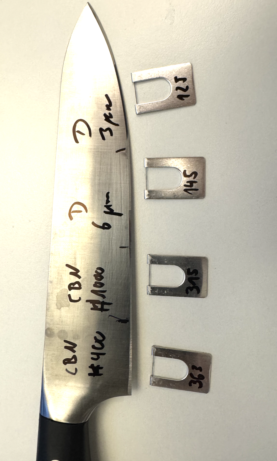
    At this point, I decided to go down the rabbit hole and get a couple of wheels that are considered “high end”. Mainly, a #400 Grit CBN wheel, a #1000 grit CBN wheel (both galvanic bond), and a 6 micrometre and 3 micrometre diamond wheel (both resin bond). And while they make a very pretty and glossy surface, and a sharp knife edge, I was curious to dig a little deeper into how the surface looks like.

    For this, I prepared a knife with increasingly finer edge preparation. First, only the #400 grit CBN wheel, then a section of the blade with #400 and then #1000; followed by a section going through the two CBN wheels and then the 6 micrometre diamond wheel, and then at the very tip, all wheels down to the 3 micrometre diamond wheel. The knife used was a cheap “IKEA” knife from stainless steel. I choose 19 degrees per side (DPS). You’ll see in a moment why I choose a cheap knife.

    The following gallery shows optical microscopy micrographs of the cutting edge quality:

    Optical microscopy shots of the cutting edge prepared with #400, #100 grit CBN, as well as (darker colored, smoother) 6 micrometre and 3 micrometre (nearly “flawless” at this magnification) diamond resin wheels.

    I then cut the blade apart, and analysed the cutting edge quality in the SEM.

    The cutting edge after the #400 grit CBN wheel. SEM micrographs show an overview, the surface morphology in the middle of the cutting chamfer as well as a detail view of the cutting apex.

    This piece of the blade measured in at 363 bess. The resulting BESS media looked pretty torn up:

    The #1000 grit CBN wheel, which is often considered the “finest” sensible CBN wheel, left a much nicer finish:

    The cutting edge after the #1000 grit CBN wheel. SEM micrographs show an overview, the surface morphology in the middle of the cutting chamfer as well as a detail view of the cutting apex.

    The BESS measured in at 315, and the media looks much smoother cut:

    With the 6 micrometre diamond wheel, the finish is starting to approach the resolution limit of this small desktop SEM, as it becomes smooth enough to be nearly flat.

    The cutting edge after the 6 micrometre diamond resin wheel. SEM micrographs show an overview, the surface morphology in the middle of the cutting chamfer as well as a detail view of the cutting apex. Note the two additional images at a higher magnification to showcase the burr formation.

    The BESS value clocked in at a respectable 145. The media is nicely sliced:

    The final “polish” was done with the 3 micrometre diamond resin wheel. This one already exhibits quite a bit of pressure, and doesn’t remove a lot of material.

    The cutting edge after the 3 micrometre diamond resin wheel. SEM micrographs show an overview, the surface morphology in the middle of the cutting chamfer as well as a detail view of the cutting apex. Note the two additional images at a higher magnification to showcase the burr formation.

    The BESS score clocked in at 125. The media is properly cut:

  • Introduction

    Welcome, Fellow interested!

    This Blog is meant as a more permanent resource to some of the things I come up with. It features endeavours in machining, milling, and manufacturing, but also in all things science, microscopy, innovative and probably also some things that I just find plain awesome and want to share.

    This block is my personal opinion, but in a time where anyone can be a source, and a lot of generated, wrong or half-truths are around, I feel the need to briefly introduce myself, set a couple of ground rules and make clear why you maybe want to believe what you are seeing here.

    My professional background and day job is Head of Future Technology at Kern Microtechnik GmbH, a Germany based machine tool company that builds probably the most advanced and precise 5 axis milling machines on the planet. My work there looks into developing radically new ideas, how material can be removed. I encounter materials daily that most people only have a bare idea about. A typical week features ceramics, high tech alloys and weird materials such as commercially pure Molybdenum. I am very fortunate to have a fantastic set of equipment there, from an awesome machine to world class, national lab grade metrology equipment. Whenever I feel the need, I dabble in technical marketing and sometimes just mill cool stuff.

    Academically, my background was formed at the Technical University of Darmstadt. While probably the hardest time in my life, I have very fond memories of my alma matter. I’ve done my Bachelor of Science in Electrochemistry (Synthesis and Characterization of CoFe Nanowires), my Master of Science in Material Science (Process analysis of burnishing in hardened stainless steel) and my PhD (Dr.-Ing.!) in Material Analytics (Experimental Investigation of Milling with geometric defined cutting edge in hard, technical ceramics). I’m currently pursuing a Doctor of Business Administration with the focus on marketing.

    Personally, I like to tinker in my freetime. My current super-fixation is knife sharpening. I’ve been very fortunate to have good friends that helped me get into this.

    I’d like to set some ground rules, also for myself:

    1.) This is my personal opinion.

    2.) This blog is independent. It’s impossible to buy or influence my opinions stated here.

    3.) Whenever I do not know something, I’ll state this. Probably through “I’m not sure, but I think…”

    4.) Whenever something is not real (e.g., drawn, simulated or AI generated) I will specifically mark this. You can be very sure, that every word you read, every post and every sentence is typed by a human being – yours truly!

    5.) When we hit a point where we are liable to get into conflict with professional IP, especially of my dayjob, I’ll state so and not continue onwards.

    And last but not least: I firmly believe in the scientific method. A lot of the content you will see is done how a 18th century physicist would do it: Make an experiment, do an observation and then draw conclusions. I’m equally form in: if you didn’t measure it, you didn’t do it.

    So long,

    Dr. Marv