Category: Allgemein

  • A brief study on sharpening stones – Part 8 – Stropping Leather and Stroppy Stuff (1 Micron)

    This is part of a series of blog posts – looking into the appearance and composition of commercially available sharpening stones. If you are interested in the previous episodes, check out the archive for them.

    If you have some suggestion on what I should look at next, or want to share your super secret DIY stones, I could be persuaded to open the bag of analytical devices… hit me up on Instagram under @marvgro for that.

    Disclaimer: I’m not for sale. Every review you see on this blog is bought with my own money. I have no affiliation to any manufacturer.

    Review

    Today we’re going to take a look at 3 different leathers, and what is considered the world’s finest stropping compound – Stroppy Stuff, in the 1 micron size.

    The idea behind stropping is to refine a cutting edge. With sharpening stones, what you are doing is mostly grinding – your cutting abrasive is fixed in place. With stropping, your cutting abrasive (the compound) is able to move around, but preloaded with force – this would be considered lapping in the engineering world.

    The leather I have here is a very flesh, cheap bovine leather (sold by Schleifjunkies, a German reseller of sharpening equipment), and a thin, high end Kangaroo leather. Because I find it hard to spell, we’re going to call it Mow-leather respectively Roo-leather for the rest of the blog. The mow-leather we’re going to look at two sides, the flesh and the grain side. Because I have very little clue about which is which, I asked Max from Stroppy Stuff to identify it for me, and Lars, a sharpening ninja from Canada helped me.

    Let’s take a look at the leather under the microscope!

    Optical micrograph of the Roo-leather. Notice the fine grain and marmoration. Scale bar is visible in the lower right of each picture. Instrument: Leica Emspira.

    The Roo-Leather is very fine and thin. It flexes just barely, and has a nice, fine composition. Leather is mostly collagen fibres, which are heavily artificed via chemical processing. A good introduction to this is chapter 3 in the book “Chemical Testing of Textiles” by Q. Fan, published by Elsevier in 2005.

    Next, we’re going to take a look at the Mow-leather, the flesh side:

    Optical micrograph of the Mow-leather, flesh side. Notice the coarser overall structure, and black particles.

    It is coarser than the Roo-leather. The German reseller of this piece of leather likes to produce large, soft, junky pieces. They give a lot, so extra care needs to be taken to not push down with the edge, or convexing will inevitably happen.

    Lastly, let’s take a look at the grain side of the Mow-leather:

    Optical micrograph of the Mow-leather, grain side. Notice the coarser overall structure, and black particles.

    It is coarser than the Roo-leather, but finer than the flesh side. The black sprinkles are more visible here.

    Typically, leather is treated with stropping compound to raise the abrasive effect. Widely considered the best compound is stroppy stuff – it’s ultra high concentration (we will later see that this is true in our SEM analysis!), finely dispersed (also true!) and it is a compound that doesn’t leave you with a slimy film after it dries. I think that property alone is worth it.

    Let’s start by looking at these things under the SEM. If you are unsure about what you are seeing here, I wrote an introductory post about the SEM analysis, which explains things in depth.

    SEM micrographs of the grain side of the Schleifjunkies leather. Note the density & large prismatic particles. Instrument: Zeiss GeminiSEM560.

    The grain side of the schleifjunkies leather shows large, flat areas, intermixed with fibrous sections. In the fibrous sections, there are prismatic particles. These can be identified via EDS as calcium oxide, a chemical which is often used for treating leather. Funnily enough, some of these are a perfect representation of the crystal structure of CaO, compare the wikipedia article for a picture of that.

    EDS analysis of the leather and the particles. Instrument: Oxford Ultim Max  ∞ 40mm2 EDS sensor. Note that our EDS sensor doesn’t show elements lighter than boron.

    Let’s take a look at the flesh side, as it’s not sanded:

    SEM micrographs of the flesh side of the Schleifjunkies leather. Note the density & large prismatic particles. Instrument: Zeiss GeminiSEM560.

    This side is much coarser, with thick fibres. and large particles embedded in it. This is probably the black particles visible in the optical micrographs. I’d guess that this is SiC from the grinding processing of the leather during manufacturing.

    Let’s take a look at the Roo-leather. It’s supposed to be a much better stropping base.

    SEM micrographs of the Roo-leather. Note the overall thicker fibres. Instrument: Zeiss GeminiSEM 560.

    I’m quite surprised. instead of many small fibres, we have larger fibres, and a stacked, layered build up. Really cool! This explains why it’s so soft and yet so strong.

    A piece of this Roo-leather was treated just like Max from Stroppy Stuff is explaining in his youtube tutorial. Let’s check how well it distributes the diamonds!

    SEM micrographs of the Roo-leather, treated with 1 micron diamond compound. Note the small diamond particles. Instrument: Zeiss GeminiSEM 560.

    The distribution in the flat areas is superb. Near protrusions, we find a bit higher density. In voids, there is very little particles visible. I think his method is spot on – this is a very nice result for a mechanical distribution, if one aims for a monolayer (like one does in stropping). As the voids will not have contact with the knife edge, I do not see any deteriorate effect when the abrasive is missing here.

    I was curious to see the grain shape and size distribution of the stroppy stuff diamond emulsion, but also the concentration. For this, I placed a single drop of emulsion on a 5×5 mm silicone wafer. The emulsion was then evaporated inside a vacuum chamber (0.93×10⁻³ bar).

    SEM micrograph of the dried stroppy stuff emulsion. We are left with a thin layer of hydrocarbons on the silicon wafer, and the actual grains. Instrument: Zeiss GeminiSEM560.

    This is actually a really nice concentration. I did not expect this many diamonds! Cool. The diamonds are more angular than blocky, which makes them sharper. Size distribution is pretty good, with about a single digit percentage of outliers. All of them appear to be slightly oversized. I work professionally a lot with diamond powder, this is not really surprising to me at these powder sizes. I’d say this is a high quality raw diamond material, that only with lab grade diamond powder could be improved – but that would probably tripple the cost of the emulsion.

    I wanted to quickly check whether every particle is really diamond, or if there are foreign particles. But also, whether the emulsion or colour in this one left any residue that we would not want on our knife. For this, we will use EDS again.

    EDS analysis of the dried stroppy stuff 1 micron emulsion. Instrument: Oxford Ultim Max  ∞ 40mm2 EDS sensor. Note that our EDS sensor doesn’t show elements lighter than boron.

    No foreign particles or anything besides the Carbon, some oxygen (which is probably the contamination film) and the silicon wafer are detectable. This is pure goodness, and it explains why no smearing film is left after drying. Nice job!

    I’ve a couple of points to make I noticed during the analysis of the materials.

    First, the leather does not contain silicates. None. I was not able to find a single scientific source that identified silicates in the leather. Silicates are excessively used to alter the leather, make it softer, more supple and grind it. But as far as I can tell, leather contains no natural silicates. Instead, it is mostly amino acids in the form of collagen fibres. Raman laser spectroscopy supports this. (Source: Bienkiewicz, 1983 “Physical Chemistry of Leather Making”, Krieger Publishing)

    Second: I prepared the stroppy emulsion on the leather in a well ventilated room. The rest of my roo-leather was lying on a second table in this room. Still, we can find diamond particles on it:

    SEM micrograph, focusing on some diamond particle contamination on the “untreated” Roo-leather. Instrument: Zeiss GeminiSEM560.

    I think it is absolutely imperative, to keep your strops VERY separate and clean. If you have a bunch of these lying on top of each other, you are very likely introducing scratches into your sharpening.

    Third: Leather is a natural material. There seem to be massive differences in quality, and sourcing good leather also appears to be a major task.
  • Metrology Marvels – Part 1 – Introduction to scanning electron Microscopy

    Metrology Marvels – Part 1 – Introduction to scanning electron Microscopy

    This is part of an ongoing blog series about metrology. It explains physics, principles and use cases of modern metrology devices.

    TL;DR: Explains how a SEM works. Deep dive into the electron-beam interaction, showing how every sensor gives a different picture and what they could be used for. Lot’s of solid state physics, but in the fun “look at how amazing nature is” way, not in the “equations of horror and despair” way. This should be a fun read and easily understandable, even if you haven’t thought about physics since school.

    From the amount of scanning electron microscope (SEM) pictures in this blog, you can guess that I’m a huge fan and heavy user of these wonderful devices.

    Brief historical overview & resolution limit

    The basic idea behind a SEM is the Abbe diffraction limit of resolution. Ernst Abbe was a pretty cool dude – he lived in Germany during the late 19th century. He defined the foundations of modern optics, had a very impressive beard and is credited with owning Carl Zeiss for some time and the creation of Schott AG. In precision engineering, he has had a lasting impact, mostly for his definition of Abbe Error Compliance (Measurement device in axis of movement is more precise than parallel to axis), but also the Abbe diffraction limit.

    It basically states, that the minimum resolvable feature size d is a function of the wavelength of your radiation λ divided by 2 times the index of refraction of the immersed medium n (for example air) times the half-angle subtended by the objective lens θ. The numerical aperture NA describes the resolving power of a objective lens, and is the product of n * sin θ. Thus we have for our system resolution:

    d = λ / 2 NA

    If you have air between your objective lens and sample, NA can only ever be below 1. Very high quality, large magnification objective lenses can for example have 100x/NA 0.95, coming very close to this theoretical limit. This means, at absolute best, our smallest, resolvable feature is about half the wavelength of the radiation. If you have a nice, confocal microscope, your system might use a green LED at 532 nm, thus your systems resolving resolution is in the range of 0.25 µm. There’s a couple of techniques to get around this limitation, but with visible radiation, you are not going to get massive improvements in lateral resolution. But: the wavelength of radiation is inversely proportional to the energy of the radiation:

    E = h*f and: λ = c/f

    Visible light typically has an energy of 0.5 – 3 eV, a WLAN signal about 5 µeV. X-Rays start somewhere around 1 keV, and most SEM have their resolution sweet spot at 15-30 keV. Modern tunneling electron microscopes TEM are in the range of 200-300 keV. Sadly, we do not have a TEM at Kern Microtechnik GmbH. *chicken scratches one onto the “Dr.Marv purchase wishlist”*

    The first instrument that can be considered a SEM was build by the German Manfred von Ardenne in 1937. His patent is still online in the European patent space, and a wonderful read.

    Now, the actual resolution of a SEM isn’t as close to the theoretical limit as optical microscopy has, because it is surprisingly difficult to compensate all beam and lens (magnetic field) errors. Aberration error correction is something that is only now really hitting the market.

    Nevertheless, even a small, entry level desktop SEM like our Thermo Fischer PhenomXL spots a datasheet resolution of smaller than 10 nanometre. Typically, this is achieved as the distance between gold nanoparticles on carbon. Very conductive, maximum elemental contrast and clearly defined boundary edges. It goes without saying, that this is the easiest possible image for a SEM!

    SEM micrograph of a very dirty, hydrocarbon contaminated resolution test object. What you see is gold nanoparticles on carbon, at a very high magnification (500kX) and very low accelerating voltage (1 keV). Analysis has shown that our instrument is within specification, even here: 0.7 nm @1keV. Taken with the magnificent Zeiss GeminiSEM560.

    At lower energy, the electrons are also much slower, thus experiencing more extraneous influences such as magnetic stray fields or vibrations from body or acoustic noise. A high resolution SEM will have sub 1 nanometre resolution over the entire energy range.

    General working principle of a SEM

    We have defined that instead of using a beam of visible light, an electron microscope uses a beam of electrons to look at matter. At minimum, an electron microscope consists out of an electron source, some condenser, scanning and focusing “lenses” (which are actually coils with a magnetic field), an aperture, a vacuum chamber with the sample as well as a sensor to detect the signal.

    Below is a schematic view of the column design of our ultra high resolution, Zeiss GeminiSEM560.

    Schematic cross section of a high resolution SEM column. Pictured detector is a SE2 Everhart Thornley type.

    At the electron source, electrons are generated. There’s two typical ways: thermionic emitters, where either a tungsten or a LaB6 filament is heated until free electrons are emitted. The second option is a field emission gun (FEG), where a small filament is heated, but the electrons are removed via a strong electric field. FEG are typically more stable, have less noise and a narrower energy spread. They are more expensive and set higher requirements to the vacuum system.

    The electron beam is then accelerated via an electric potential, and then shaped and focused via condenser lenses. The beam current is regulated via an aperture orifice. The beam is then focused and scanned across the sample in a regular pattern via the objective lens. This scanning is not a continuous process, but instead the beam dwells for a short amount of time at every “pixel” position. A detector simply counts the signal emission at every point, thus creating a black and white picture from the sample – electron beam interaction.

    It is a very basic principle, but the interaction of the beam and the sample is very complex, and many sensors exist to detect different types of signals. What is really nice about this scanning and way of detecting a picture compared to having a high resolution sensor with many pixels is that all sensors have the same focus point – so you can typically seamlessly switch between sensors and don’t have to refocus.

    Electron – Matter – Interaction

    In order to understand the different pictures and data created from a SEM, we need to take a quick detour towards high-energy electron beam interaction with matter. When matter is hit with fast electrons (the primary electrons, PE), a couple of possible interactions can happen. The below schematic shows the 4 dominant types, mainly back-scatter electrons (BSE), secondary electrons (SE, type 1 and 2) and x-ray emission (hv). The interaction volume depends on beam energy, but is typically in the range of < 10 nm for SE1, 1-50 nm for SE2, 50-1000 nm for BSE and 1-10 µm for hv. Because of scattering, the interaction volume is shaped a bit like a pear.

    Schematic beam interaction with matter. The 4 main emitted signals are shown: BSE, SE1, SE2 and hv.

    The interaction volume depends on beam energy, but is typically in the range of < 10 nm for SE1, 1-50 nm for SE2, 50-1000 nm for BSE and 1-10 µm for hv. Because of scattering, the interaction volume is shaped a bit like a pear. To show this interaction, I’ve prepared a small Monte-Carlo scattering simulation highlight this interaction volume, and how deep the different species might reach. This is for a high energy beam in a light material.

    Interaction volume of high energy electrons in a light material. SE are highlighted in green.

    We will have to dig a bit deeper into the creation of each of these, but also how they change the picture and what data and conclusions we can draw from them. For this, I’ve put a very used, nearly broken carbide end mill into the SEM.

    First/left picture: The used endmill, before being inserted into the SEM chamber. Second/Right picture: the inside of the chamber, with the visible polshoe, SE2 detector and illuminated chamberscope. A couple more complex sensors are visible in the background.

    After pumping the chamber empty of air, activating the SE2 sensor and focusing, we can generate an overview image of the tool. Because the SEM flares the field at the objective lens, we get a much larger FOV, but heavy distortions. This is mostly useful for navigating and finding a feature (or even: where the heck am I currently!).

    SE2 overview picture of the inserted endmill. Instrument: Zeiss GeminiSEM560

    Secondary Electrons

    Sometimes, when the incident electrons interact with an atom, they do so through inelastic scattering with the shell electrons. This ionises the electron, via ejecting a shell electron, the so called secondary electron. If it’s the primary electron, these SE are called SE1, and are very surface sensitive and detected via a SE detector inside the electron column. If it’s created by backscatter electrons ionising the atoms, they are called SE2 and are detected via an in-chamber detector. These are very sensitive to topography, so the resulting picture is a good representation of the shape and surface of the sample. Because they are created by BSE, the interaction volume is a bit deeper, and the signal can’t resolve very fine surface detail. This sensor is very susceptible to static charge up on the sample.

    Schematic depiction of the SE creation process. Note that the incident species can also be BSE, and not only SE.

    The SE2 sensor is very fast in it’s readout speed, and typically, especially at longer working distances (distance between the pole piece and the sample) exhibits a strong signal. If the sample is non-conductive, this is my first choice in focusing the picture and for navigating. Because it is at an angle inside the chamber, the sensor gives a very good depth representation of the sample. Pictures look plastic and 3 dimensional.

    SEM micrograph of the cutting edge. Signal A = sensor used, in this case the chamber SE2 type. The picture has depth, and nicely shows the morphology of the grinding marks, the coating and particles on the tool.

    Switching to the InLens SE1 detector, the picture changes in it’s appearance:

    SEM micrograph of the cutting edge. Signal A = sensor used, in this case the InLens SE1 type. The picture has lost some depth, but gained some detail on the surface structure. Besides the grinding marks, the micro-roughness of the coating is now visible.

    Because this sensor has a very small interaction volume, it shows fine surface details. Whereas the SE2 sensor mostly showed the grinding path along the tool cutting edge, this sensor shows the micro roughness of the coating, and highlights different sections of the build up edge through finer detail. At the same time, some depth perception is lost, resulting in a flatter picture.

    Back Scatter Electrons

    Back scatter electrons are created from elastic scattering (reflection) with the nucleus of the atoms. Because of this, the electrons have a lot of energy. The chance for elastic scattering depends on the mass of the nucleus, thus heavier elements give you a brighter signal. Therefore, the BSE signal gives you a material contrast.

    Schematic depiction of the SE creation process. Note that the incident species is either the PE, or a lower energy already back scattered BSE.

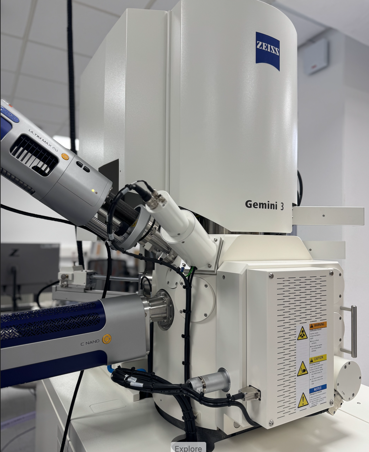
    The same cutting tool we looked at in the SEM can also be visualised with back scatter electrons. For this, our GeminiSEM560 is equipped with two different one: the ESB detector, that sits very high up in the column, and a retractable diode type 4 sector BSD sensor that can be fitted exactly below the pole piece.

    Because we can always activate it, let’s start with the ESB detector picture. We can see that the image is flattened a lot – this sensor is not really picking up any topography.

    In column ESB detector SEM micrograph of the cutting edge. Note the lighter coloured structures – these are heavier elements than the darker coloured structures.

    This sensor is quite “slow”, in the sense of it not getting a lot of signal. The above picture took a bit over 4 minutes to record.

    The SEM is fitted with a diode type, 4 sector BSE detector, that can be retracted and inserted via a pneumatic cylinder. Because it is sitting below the pole piece, it is much quicker, and still shows some surface structure.

    Chamber BSD SEM micrograph of the cutting edge. The picture has very little depth, showing only a minimal amount of surface structures. The BUE material is clearly distinguishable, showing 2 different materials via the inherent BSD material contrast.

    This sensor is much quicker, and shows some topographic details. A bit more depth perception than on the ESB sensor is given.

    X-Ray creation (EDS – Energy dispersive x-ray spectroscopy)

    The PE are able to create x-rays. I find this absolutely fascinating, and one of my favourite tools inside the SEM. When the PE interacts with the atomic shell, sometimes an electron is ejected (the SE). If this happens at a lower shell, a hole (missing electron spot) is created. Because most systems strive to lower their potential energy, a higher shell electron will then drop down. Because the new orbit has a lower radius, there is now some excess energy. Through this energy, just like Einstein foretold, a particle is created, specifically a x-ray photon. Because the distance between shells is dependent on the weight of the atomic core and it’s configuration (proton number), the energy difference is unique for every element.

    Schematic description of the x-ray creation process. An incident electron creates a hole in an inner shell through inelastic scattering (a SE is ejected). A higher shell electron drops down to fill the hole (blue arrow), because of energy conversion the lower orbit energy results in the creation of a x-ray photon.

    By recording lots of x-ray photons, and sorting them by their inherent energy, we can identify and map an elemental distribution over our picture. This process is called energy dispersive x-ray spectroscopy. It doesn’t tell you “This is REX 121 steel”, but instead after several minutes you can say “oh, we have about 12 % chromium in our sample. Maybe. I hope. Pinky promise!?”. This is the part where TV shows have ruined science for us scientists. But if done right, at correct readout sampling rates, high beam energy, you get fantastic results.

    What can we see on our tool edge? First and foremost the coating material – Ti, Al, N, Cr, resulting from a ceramic high tech multi layer coating applied to most modern tools. Build up edge and particles from aluminum, some stuck carbon, places where the coating has failed and tungsten carbide is visible through the coating. Pretty nifty, eh?

    EDS analysis of the tool edge.

    The real expertise in EDS is looking at the data and then making judgement calls and drawing from experience and know how. We once found a particle we wanted to analyse, and it contained bromine. People were stumped, because which part of the machine contains bromine? In the end it was the base of our powder coating, and the particle we found at a place it shouldn’t be was the powder coating from the machine enclosure that had flaked off. We managed to nail that down, because the only reasonable expectation of where bromine could be used was exactly that. Comparing a fresh piece revealed identical chemical composition.

  • Abrasive Snippets – Part 2 – CBN Grains (8-12 micrometre)

    This is part of a series of posts about abrasives. This is mostly cool SEM pictures, but I find them interesting. It’s quite difficult to image small grains at large magnifications, so there’s very limited information and pictures online about them.

    This post is about 3 different CBN abrasives. They are all nominally 8-12 µm sized. Curiously, they are different colours. Manufacturer: Ceratonia, Germany.

    The first type is an amber coloured one. It’s blocky, and supposedly very nice lapping of steels or galvanic applications.

    SEM micrographs of 8-12 µm CBN grains, amber coloured. Instrument: Zeiss GeminiSEM560.

    The second time is a black one, supposedly self sharpening and ideal for super alloys and hardened steels.

    SEM micrographs of 8-12 µm CBN grains, black coloured. Instrument: Zeiss GeminiSEM560.

    The third type is a brownish coloured one. I managed to pour half of my sample over myself, nice work Dr.Marv. Monocrystalline and very hard.

    SEM micrographs of 8-12 µm CBN grains, brownish coloured. Instrument: Zeiss GeminiSEM560.