Category: Allgemein

  • A brief study on sharpening stones – Part 6 – Edge Pro Matrix Stone 4000 Grit (5 micron diamond, resin)

    This is part of a series of blog posts – looking into the appearance and composition of commercially available sharpening stones. If you are interested in the previous episodes:

    Part 1 is about the Fällkniven DC3 , Part 2 is about the DMT mini W7C, Part 3 is about the TSPROF Blitz F1000, Part 4 is about a natural jade stone, Part 5 is about the Venev 5/3 Diamond Resin Stone.

    If you have some suggestion on what I should look at next, or want to share your super secret DIY stones, I could be persuaded to open the bag of analytical devices… hit me up on Instagram under @marvgro for that.

    Today’s sharpening stone is the Edge Pro Matrix Stone at 4000 grit, which according to the manufacturer equals 5 micrometre grain size. It’s their stone “made for modern super steel” and apparently self sharpening by loosening grains over time. 🙂

    It’s a super smooth, very fine stone. Stroking it with your finger, it just feels barely sticky, while scratching it with your fingernail shows some resistance – but can also leave a small groove.

    Optical micrographs of the Edge Pro Matrix Stone (4000). The scale bar is visible in the lower right corner. Instrument: Leica Emspira.

    The microscope supports this picture. A very uniform, smooth surface. The corners around the stone are slightly beveled. At higher magnifications, grains start to become visible. Do we have a new king of agglomeration here? Let’s throw it into the SEM to check it out.

    The first thing I saw in the SEM was…nothing. Because this stone is so smooth, and also because they really seem to use no fillers, additives or anything else, it immediately starts charging like crazy. The resin they are using is also covering the topmost layer, making it hard to distinguish between resin and diamond. Well, this ain’t a BEAST of a scanning electron microscope for nothing. We’ve equipped it with multiple sensors and it is a very versatile device. To make an image visible, I’ve bumped up the accelerating voltage. To explain why this is different to the other pictures you’ve seen in this blog before, I think I need to detour for a small moment.

    In a scanning electron microscope, the image is created by using a beam of electrons, and moving that one in regular lines across the surface of a sample. At every point it hits the sample, interaction happens. This interaction is typically either an elastic reflection of the incident electrons (back scattered electrons, BSE), or the ejection of electrons from a shell around the atoms (secondary electrons, SE). The BSE are showing you mostly elemental contrast, whereas the SE show you a topographical (surface) contrast. Nevertheless, with good enough sensors, both show you a bit of the information of the other type. Now, the BSD (back scatter detector) is pretty robust, and works nicely at lower vacuum. Because the sample is non conductive, it will experience static charge. Lowering the chamber vacuum introduces moisture (H2O) into the chamber, and this is enough to reduce the static charge on the sample. Unfortunately, lower vacuum also means lower resolution, and the BSD doesn’t give us great surface morphology to begin with. A workable way to combat this is to increase the accelerating voltage. This will not only give you more signal, reduce noise, but also increase the interaction volume of the beam. Basically, you are now looking a couple micrometre deep into the material!

    SEM Micrographs of the Edge Pro Matrix Stone (4000). Note that these pictures are BSD and at high accelerating voltage. Instrument: Zeiss GeminiSEM560.

    We can see that this stone really only contains a matrix and the diamond grit. All grains are small with tight controlled size distribution. No fillers or other abrasives are visible. The matrix is relatively dense, and the atomic contrast of it is similar to the diamond next to it. This is the first stone I’ve looked at that contains no fillers. Unfortunately, with this comes two problems: Quite a bit of agglomeration is visible, with often 3 or more grains sticking close to each other. The second is the retention of the grains – we can see on this unused stone already, that nearly no grain is sticking out of the surface. Even the manufacturers dressing process removed the majority of all surface grains. I would expect this stone to be quite slow and soft. Because of the simple composition, no EDS was recorded.

    The surface under the white light interferometer shows a smooth, regular and low roughness surface.

    White light interferometry height map of the Edge Pro Matrix Stone (4000). Instrument: Zygo Nexview NX2, Objective Lens: 10X. Stitched overview of 4×4 images.

    The overall height distribution is lower than for example on the similar grit Venev stone. The actual contact surface, at least brand new, should be relatively low, as it doesn’t show a lot of plateaus in the height map.

    ISO 25178 parameters of the Matrix Pro Stone (4000).

    The areal surface parameter support this observation. This is one very smooth stone, with very low roughness and material ratio.

    In order to evaluate the sharpening performance of these stones, 3 blades were sharpened. In order to evaluate the sharpening performance of this stone, a blade was sharpened with it. I am using a standardised testing procedure, read about it here. Nevertheless, it’s 65 HRC M398, and sharpened to 17 DPS with resin bond diamond stones down to 10 µm. Afterwards, the tested stone is used, first in a back and forth movement until the surface becomes homogenous, and then alternating, edge trailing strokes (5-5-3-2) on each side, for a total of 20 strokes per side. No pressure is applied but the weight of the apparatus. Then the Pro Matrix stone comes into play.

    SEM micrographs of the sharpened blade. Note that the last picture (2kx magnification) isn’t a center zoom of the one before, but slightly to the left of the FOV, as I identified some carbide cracking that I wanted to visualise in higher detail. Instrument: Thermo Fischer PhenomXL Scanning Electron Microscope.

    The surface of the edge is much smoother than with the equally sized Venev sharpening stone. The edge shows a low waviness and no identifiable burr. This is certainly a statement to the heat treat of the steel (made by Roman Kasé!), but also to the stone. Some deeper grooves are visible, which could be because of the agglomeration, or a rolling grain that got loose. The low material removal rate gives a high cutting pressure, likely leading to the carbide cracking and edge breakouts at carbide-steel interfaces. This is a cool stone, with a nice feeling while sharpening, awesome result and very finely made. I like it. If only it was a faster stone!
  • A brief study on sharpening stones – Part 5 – Venev Double Sided Diamond Stone 5/3 Side

    A brief study on sharpening stones – Part 5 – Venev Double Sided Diamond Stone 5/3 Side

    This is part of a series of blog posts – looking into the appearance and composition of commercially available sharpening stones. If you are interested in the previous episodes:

    Part 1 is about the Fällkniven DC3 , Part 2 is about the DMT mini W7C,

    Part 3 is about the TSPROF Blitz F1000, Part 4 is about a natural jade stone.

    If you have some suggestion on what I should look at next, or want to share your super secret DIY stones, I could be persuaded to open the bag of analytical devices… hit me up on Instagram under @marvgro for that.

    Today’s sharpening stone is an artifical, resin bound diamond stone. I believe these are sold under the TSPROF brand, but are made by Venev and are made by Venev, too. While it has two sides, for comparisons sake I only looked at the 5/3 micron side in detail. Why does it have two numbers here? Well, getting a very tight control on the grain size is expensive. Up to a certain size one can sieve it, and there you’d obviously have a spread of sizes (basically: everything that was smaller than the last sieve you used, but larger than the current sieve you are using). At a certain grit size though, this process is replaced by sedimentation. You basically dump your diamond powder that is created by crushing larger diamonds against each other into a tank with water, stir it vigorously and then leave it standing. Heavier particles sink to the bottom quicker than lighter ones, so you then suction it off layer by layer. The more careful and skilled one is at this process, the tighter the size distribution is. Typically, asia-sourced diamond is pretty good at this. Nevertheless, 5/3 is a very honest way of describing it. In Germany, tightly controlled (and lab analysed & certified!) diamond powder is readily available, but about 20 times more expensive than foreign sourced one. We should therefore expect to have a wide range of different grain sizes in this stone.

    Taking a look under the optical microscope, a mix between reflective grains, darker but also green grains and a reddish matrix is easily identifiable.

    Optical micrographs of the Venev double sided 5/3 micron diamond stone. The scale bar is visible in the lower right corner. Instrument: Leica Emspira.

    It would be quite interesting to see what grains are diamond, what the other ones are (or if all are diamond!) but also what the surface microstructure looks like. For this, the scanning electron microscope is king. The resolution and depth of focus is just so nice. As this is a 1″x6″ stone, off it goes into our fantastic Zeiss GeminiSEM560. Absolute overkill, but it fits, so we here we go:

    SEM Micrographs of the surface morphology of the Venev 5/3 micron diamond stone. Instrument: Zeiss GeminiSEM560.

    The manufacturer says that they are using an organic bond, based on phenol-formaldehyde resins. These are typically improved by adding various fillers to them, for example SiC (to make it harder), copper (to improve heat transfer), but also organic material such as woodchips or fabric fibre to improve tensile strength. Information from the manufacturer about this is a bit inconclusive – apparently, they have a “B2-01” bond, that has fillers, and an improved “OSB” bond, that should not have “boron carbide” in it. Apparently the finer stones, such as this one, have the improved bond. What I find curious at this point is that the above SEM pictures show a large variance of grains – some, that would fit in the 5/3 micrometre range, but others that are much larger, and of a lighter colour. The SEM is special in terms of microscopes, in that every picture not only contains topographical information (e.g. the surface appearance), but depending on the sensor also some chemical information. The sensor used for the pictures above is the “SE2” sensor, which detects secondary electrons. These are created in the beam-matter interaction by basically hitting an electron on the atom-shell, and shooting it out. It is a very surface sensitive detector, mostly showing topography. Nevertheless, if you have much heavier elements, you get a very slight elemental contrast. The large grains are slightly lighter grey than the smaller grains, which could point towards them consisting out of heavier elements, for example SiC instead of C which would be found in pure diamond.

    Fortunately, the SEM is equipped with a sensor to identify elements.

    EDS analysis of the Venev 5/3 micron diamond stone. Instrument: Oxford Ultim Max  ∞ 40mm2 EDS sensor. Note that our EDS sensor doesn’t show elements lighter than boron.

    As postulated above, the abrasive in this stone consists out of some large, 10-15 micrometre sized silicon carbide (SiC, pink colour) grains, but also some agglomerated magnesium-oxide particles (MgO, green colour). The diamond grain concentration looks to be about C100 (equaling 25% by volume, but the standard is pretty vague on how and when this is determined). Nevertheless, I’m a bit disappointed by the mixing here – it seems like we have several agglomerated nests of diamond, with some spare grains in between. Also, I would imagine one will have quite the large scratches from the large SiC particles. SiC typically reaches a hardness of 2500-3000 HV, much harder than a decent powder metallurgical steel would achieve (64 HRC are around 800 HV, CBN is at 4000-5000 HV, diamond at 10000 HV in it’s hard crystallographic orientation). MgO meanwhile comes in at 1200 HV. In subtractive manufacturing, the typical rule of thumb is: your abrasive should be 5 times harder than the workpiece. Otherwise, you will have excessive wear on it. The binder clearly is organic in origin, a phenol based one seems likely by the appearance and “brittleness” of it. If you ask me, this was baked at a bit too high of a temperature, and with not enough pressure. This could explain the “debris type” dusting on it, as well as the large voids.

    Taking the stone for a look under the white light interferometer, we can see the surface structure is very regular, but also quite coarse.

    White light interferometry height map of the Venev 5/3 micron sized stone. Instrument: Zygo Nexview NX2, Objective Lens: 10X. Stitched overview of 5×5 images.

    I could imagine that the deep pits we are seeing are actually foaming of the phenol-resin during the curing process, and not just tear outs from the dressing process, as I haven’t identified any particles this large. Nevertheless, if you compare it with the SEM picture of the large, molten agglomeration of binder, it could also be that these are distributed all along the stone, and we see the result of these tearing out.

    ISO 25178 parameters of the Venev 5/3 micron diamond stone.

    The stone is actually, and quite surprisingly, very coarse in it’s surface. I would have expected a stone with this fine grit to have a fine, polishing surface. The roughness is actually much higher than on for example the natural jade stone we looked at the last time. Nevertheless, the shape of the surface in itself can’t be considered very sharp, as for example the Kurtosis (Sku) is only slightly above 3.

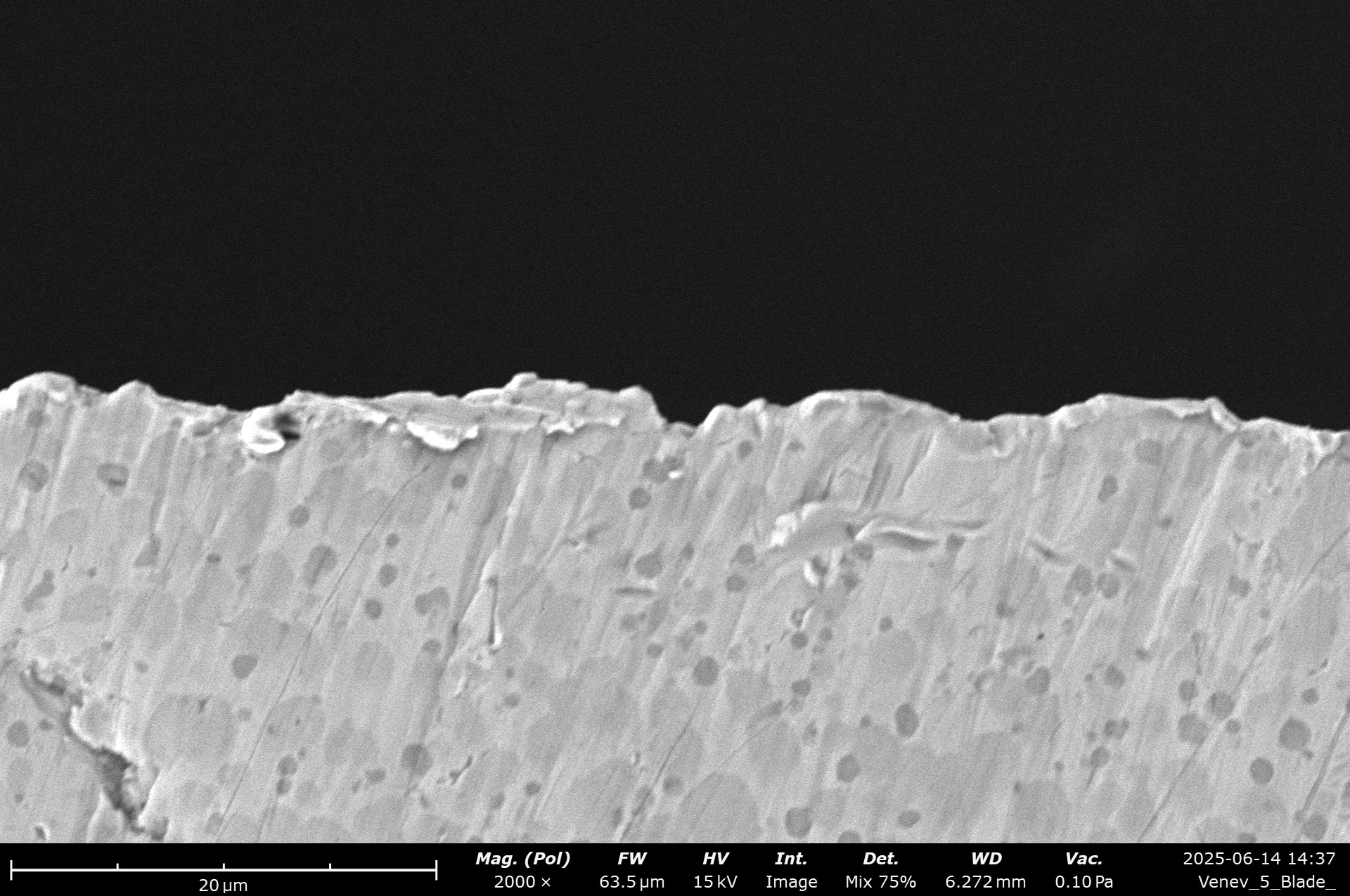
    Seeing as this is an interesting stone for sharpening, I’ve taken the trouble of sharpening a blade with this. In order to evaluate the sharpening performance of these stones, 3 blades were sharpened. In order to evaluate the sharpening performance of this stone, a blade was sharpened with it. I am using a standardised testing procedure, read about it here. Nevertheless, it’s 65 HRC M398, and sharpened to 17 DPS with resin bond diamond stones down to 10 µm. Afterwards, the tested stone is used, first in a back and forth movement until the surface becomes homogenous, and then alternating strokes (5-5-3-2) on each side, for a total of 20 strokes towards the apex per side. No pressure is applied but the weight of the apparatus. Then the Venev stone was used.

    SEM micrographs of a test blade, done with the Venev stone. Note the beautiful distribution of carbides in the M398. Boehler and Mr. Kasé are magicians! Instrument: Thermo Fischer Phenom XL Scanning Electron Microscope.

    The result is a keen edge, with burrs that are already very hard to detect under an optical microscope. The largest burr I found was in the low, single digit micrometre range. Nevertheless, there’s some heavier scratches, and the cutting edge is slightly wavy. Comparing the deeper pits at the edge, I don’t think it’s massive carbide cracking, as those are a bit larger than the very fine carbides. I would imagine this is most likely the larger SiC grains, grinding away the edge. A pity!

  • A brief study on sharpening stones – Part 4 – natural Jade

    This is part of a series of blog posts – looking into the appearance and composition of commercially available sharpening stones. If you are interested in the previous episodes:

    Part 1 is about the Fällkniven DC3 ,

    Part 2 is about the DMT mini W7C,

    Part 3 is about the TSPROF Blitz F1000.

    If you have some suggestion on what I should look at next, or want to share your super secret DIY stones, I could be persuaded to open the bag of analytical devices… hit me up on Instagram under @marvgro for that.

    Today’s sharpening stone is a natural jade stone. Jade is a natural occurring stone, that consists out of complex silicates. I believe that typically the one used for sharpening is from the pyroxene group. There, the minerals consist out of a certain formula: (XY(Si,Al)2O6) where X typically is a light metal such as Calcium, Sodium and Y typically is a heavier metal such as aluminium, chromium. I mention this, because jadeite typically is not pure NaAlSi2O6, but more likely a wild and varying mix of several elements, some maybe only in traces. Nevertheless, silicates are hard, with jadeite typically reaching around 1000 HV. This is harder than a cheap knife, but actually softer than some high carbide steels at their maximum achievable hardness. The other mineral that is commonly called jade is nephrite, which is a really complex mix of Ca2(Mg,Fe)5Si8O22(OH)2.  This is typically a bit softer, ranging from 700 to 1000 HV (hardness vickers). We’ll see whether we can identify what mineral our natural jade stone is made of later!

    Taking a look under the optical microscope, it is clearly identifiable as jade by it’s distinct, swirly white and green colour:

    Optical micrographs of a natural jade stone. The scale bar is visible in the lower right corner. Instrument: Leica Emspira.

    One can make out some distinct silicate grains, with a more whitish colour, and also some darker debris, likely swarf stuck to the surface. Jadeite is non-conducting, so we once again get to enjoy absurdly detailed pictures from the fantastic Zeiss GeminiSEM560. Because of it’s design, it excels at low voltage imaging, where one has lower charging effects.

    SEM Micrographs of the surface morphology of the natural jade stone. Instrument: Zeiss GeminiSEM560.

    The SEM pictures reveal a ragged topography, consisting out of a mix of ultra fine, debris like grains, but also larger, well formed grains. I struggle to give this stone a classification in terms of grit – the grains are sometimes in the nanometer range (compare the 2KX magnification picture), but some are also several micrometre large, up to maybe the low double digits.

    A nice question here is: what type of jade is this actually made out of? For this, we employ the EDS module of the Zeiss GeminiSEM560. With energy dispersive x-ray spectroscopy (typically abreviated EDS or EDX), one can identify the elemental composition of a SEM sample. This doesn’t mean you press a button and crime show like you get a beep and it identifies the material. It means that after a couple minutes, with the uncertainty of a couple percent, you can state “I think it contains iron. maybe.”. Welcome to science!

    EDS analysis of the natural jade stone. Instrument: Oxford Ultim Max  ∞ 40mm2 EDS sensor. Note that our EDS sensor doesn’t show elements lighter than boron.

    It’s generally a good idea with EDS analysis to compare the composition in percent (visible in the second picture above) with the colour map of where these elements appear. As the “full colour” summary image is quite hard to differentiate, I typically use that one to pick out the area or grain of interest, and then peek to the smaller, individual colour slices. EDS analysis nicely identifies that this jade stone consists out of Ca, Mg, Si, O. These are the elements found in neprhite (Ca2(Mg,Fe)5Si8O22(OH)2), so it’s pretty safe to say this is what the stone is made out of!

    One really cool thing our Zeiss is equipped with is a sensor called “VPSE”. This stands for variable-pressure, secondary electron detector. It doesn’t detect electrons directly, like a Everhart-Thornley would. If your sample is in “low vacuum” conditions, that ET-SE detector would short circuit out because the air is conducting. Nevertheless, secondary electrons are created by the electron beam-matter interaction, and those create little light flashes when they hit molecules in the low atmosphere at VP. Now, the VPSE detector has a very sensitive scintillator that detects these flashes. I’m telling you this, because if you aren’t in low vacuum, and you have a mineral sample, you can use the VPSE as a cathodoluminescence detector. Here, the electron beam sometimes creates light in the interaction with certain minerals. Sadly, with “abusing” the sensor in this way, it’s still only a black and white picture. But if your sample glows, you can make that visible.

    “abused” VPSE sensor micrograph to highlight cathodoluminescence of the jade stone. Image FOV is identical to the SE2 image earlier in this post. Instrument: Zeiss GeminiSEM560.

    Does it have any relevancy to this post? No. Is it super awesome and cool? Yes!

    In order to look at the surface of the stone, the awesome Zygo Nexview NX2 white light interferometer comes to use again:

    The jade stone while being measured on the Zygo Nexview NX2 interferometer.

    The stone shows a relatively smooth surface. The uppermost surface is actually pretty flat, with a large material ratio (bearing surface). Some deep voids are sprinkled randomly over the surface.

    White light interferometry height map of the jade stone. Instrument: Zygo Nexview NX2, Objective Lens: 10X. Stitched overview of 5×5 images.

    The high material ratio with a smooth surface is one reason why this stone feels nearly like glass – very little feedback, as the contact surface area is large, and the knife slides along it without really grabbing onto the grains. This is a stone for very low removal and mostly I would guess it burnishes a knife edge.

    ISO 25178 parameters of the natural jade stone.

    Roughness wise, this is a pretty coarse stone (Sq > 7 µm), with a sharp profile (Sku, kurtosis >> 3). Nevertheless, the topmost surface is ground pretty flat.